Based on years of Institute research, MIT spinout Kateeva has developed an “inkjet printing” system that could cut manufacturing costs enough to pave the way for mass-producing flexible and large-screen OLED displays.
Flexible smartphones and color-saturated television displays were some highlights at this year’s Consumer Electronics Showcase, held in January in Las Vegas.
Many of those displays were made using organic light-emitting diodes, or OLEDs — semiconducting films about 100 nanometers thick, made of organic compounds and sandwiched between two electrodes, that emit light in response to electricity. This allows each individual pixel of an OLED screen to emit red, green, and blue, without a backlight, to produce more saturated color and use less energy. The film can also be coated onto flexible, plastic substrates.
But there’s a reason why these darlings of the showroom are not readily available on shelves: They’re not very cost-effective to make en masse. Now, MIT spinout Kateeva has developed an “inkjet printing” system for OLED displays — based on years of Institute research — that could cut manufacturing costs enough to pave the way for mass-producing flexible and large-screen models.
In doing so, Kateeva aims to “fix the last ‘Achilles’ heel’ of the OLED-display industry — which is manufacturing,” says Kateeva co-founder and scientific advisor Vladimir Bulovic, the Fariborz Maseeh Professor of Emerging Technology, who co-invented the technology.
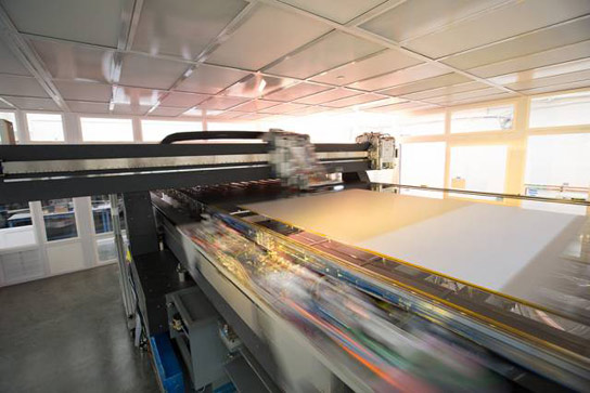
Called YIELDjet, Kateeva’s technology platform is a massive version of an inkjet printer. Large glass or plastic substrate sheets are placed on a long, wide platform. A component with custom nozzles moves rapidly, back and forth, across the substrate, coating it with OLED and other materials — much as a printer drops ink onto paper.
An OLED production line consists of many processes, but Kateeva has developed tools for two specific areas — each using the YIELDjet platform. The first tool, called YIELDjet FLEX, was engineered to enable thin-film encapsulation (TFE). TFE is the process that gives thinness and flexibility to OLED devices; Kateeva hopes flexible displays produced by YIELDjet FLEX will hit the shelves by the end of the year.
The second tool, which will debut later this year, aims to cut costs and defects associated with patterning OLED materials onto substrates, in order to make producing 55-inch (1.4-meter) screens easier.
By boosting yields, as well as speeding up production, reducing materials, and reducing maintenance time, the system aims to cut manufacturing costs by about 50 percent, says Kateeva co-founder and CEO Conor Madigan SM ’02 Ph.D. ’06. “That combination of improving the speed, improving the yield, and improving the maintenance is what mass-production manufacturers want. Plus, the system is scalable, which is really important as the display industry shifts to larger substrate sizes,” he says.
The other Kateeva co-founders and technology co-inventors are MIT Provost Martin Schmidt, now a scientific advisor; Jianglong Chen SM ’03, Ph.D. ’07, now program director; and Valerie Leblanc Ph.D. ’07, now staff scientist.
Getting flexible
TFE was invented to coat flexible OLED screens with a barrier as solid as glass, but bendable. But it is prone to contamination and other issues.
Traditional TFE processing methods enclose the substrate in a vacuum chamber, where a vapor of the encapsulating film is sprayed onto the substrate through a metal stencil. This process is slow and expensive — primarily because of wasted material — and requires stopping the machine frequently for cleaning. There are also issues with defects, as the coating that hits the chamber walls and stencil can potentially flake off and fall onto the substrate in between adding layers.
But moisture, and even some air particles, can sneak into the chamber, which is deadly to OLEDs: When electricity hits OLEDs contaminated with water and air particles, the resulting chemical reactions reduce the OLEDs’ quality and lifespan. Any displays contaminated during manufacturing are discarded and, to make up for lost yield, companies boost retail prices. Only two companies now sell OLED television displays, with 55-inch models selling for $3,000 to $4,000 — about $1,000 to $3,000 more than their 55-inch LCD and LED counterparts.
YIELDjet FLEX aims to solve many TFE issues. A key innovation is encasing the printer in a nitrogen chamber, cutting exposure to oxygen and moisture, as well as cutting contamination with particles — notorious for diminishing OLED yields — by 10 times over current methods that use vacuum chambers. “Low-particle nitrogen is the best low-cost, inert environment you can use for OLED manufacturing,” Madigan says.
In its TFE process, the YIELDjet precisely coats organic films over the display area as part of the TFE structure. The organic layer flattens and smoothes the surface to provide ideal conditions for depositing the subsequent layers in the TFE structure. Depositing onto a smooth, clean surface dramatically improves the quality of the TFE structure, enabling high yields and reliability, even after repeated flexing and bending, Madigan says.
Taking off the mask
Kateeva’s other system offers an improvement over the traditional vacuum thermal evaporation (VTE) technique — usually somewhere in the middle of the production line — that uses shadow masks (thin metal squares with stenciled patterns) to drop red, green, and blue OLED materials onto a substrate.
Much like conventional TFE processing, VTE involves placing a substrate inside a vacuum chamber, and spraying through the shadow mask a vapor of OLED material in precise patterns of red, green, and blue. But materials are wasted when the vapor is sprayed on the mask and chamber. Coating the chamber and mask can also lead to particle contamination as the material flakes off, so excessive cleaning maintenance is required, Madigan says.
This isn’t necessarily bad for making small, smartphone screens: “If a substrate sheet with, say, 100 small displays on its surface has five defects, you may toss five, and all the rest are perfect,” Madigan explains. And smaller shadow masks are more reliable.
But manufacturers start to lose money when they’re tossing one or two large-screen displays due to particle contamination or defects across the substrate.
Kateeva’s system, which, like its TFE system, is enclosed in a nitrogen chamber, precisely positions substrates — large enough for six 55-inch displays — beneath print heads, which contain hundreds of nozzles. These nozzles are tuned to deposit tiny droplets of OLED material in exact locations to create the display’s pixels. “Doing this over three layers removes the need for shadow masks at larger scales,” Madigan says.
As with its YIELDjet FLEX system, Madigan says this YIELDjet product for OLED TV displays can help manufacturers save more than 50 percent over traditional methods. In January, Kateeva partnered with Sumitomo, a leading OLED materials supplier, to further optimize the system for volume production.
Revolutionizing at MIT
The idea for Kateeva started in the early 2000s at MIT. Over several years, Madigan, Bulovic, Schmidt, Chen, and Leblanc had become involved in a partnership with Hewlett-Packard (HP) on a project to make printable electronics.
They had developed a variety of methods for manufacturing OLEDs — which Madigan had been studying since his undergraduate years at Princeton University. Other labs at that time were trying to make OLEDs more energy efficient, colorful, or durable. “But we wanted to do something completely different that would revolutionize the industry, because that’s what we should be doing in a place like MIT,” Madigan says.
Soon, however, HP pulled out of the project. “That left all this novel intellectual property sitting on a shelf that may never be used again,” Bulovic says. Instead of letting those patents go to waste, however, the researchers launched Kateeva in 2008 to commercially tackle OLED manufacturing.
A few years before, Bulovic had cut his teeth in the startup scene with QD Vision — which is currently developing quantum-dot technology for LED television displays — and was able to connect the group with local venture capitalists.
Madigan, on the other hand, was sharpening his entrepreneurial skills at the MIT Sloan School of Management. Among other things, the Entrepreneurship Lab class introduced him to the nuts and bolts of startups, including customer acquisition and talking to investors. And Innovation Teams helped him study markets and design products for customer needs. “There was no handbook, but I benefitted a lot from those two classes,” he says.
In 2009, just when OLEDs were starting to gain mainstream popularity, Kateeva launched T-Jet, a precursor to YIELDjet. In that system, nozzles would drop OLED materials onto a plate, etched with a certain pattern. The plate was heated to 100 degrees Celsius (212 degrees Fahrenheit) to dry the ink, brought close to the substrate without touching it, and heated to 300 C (572 F) to transfer the dry, patterned vapor onto the substrate. “It was a cool concept, but inkjet was still cheaper,” Madigan says.
So in 2012, Kateeva pivoted, switching gears to its YIELDjet system. Today, the system is a platform, Bulovic says, that, in the future, can be tweaked to print solid stage lighting panels, solar cells, nanostructure circuits, and luminescent concentrators, among other things. “All those would be enabled by the semiconductor printer Kateeva has been able to develop,” he says. “OLED displays are just the first application.”
Never miss a breakthrough: Join the SciTechDaily newsletter.
Follow us on Google and Google News.
2 Comments
Awesome to see a printer with an ability to expedite manufacturing efforts (and eventually costs).
No mention of OLED burnout.
My GL 55″ OLED TV has the CNN bottom red Logo/Text box leaving a ghost colour image, particularly when showing a red background.
The line from the sky fast-forward/pause also leaves a black burnout line.