Penn Engineers have innovated a thin, efficient superlattice that could significantly enhance photodetector components used in various high-tech applications, including self-driving cars and advanced computing.
Cameras, solar panels, biosensors, and fiber optics are technologies that rely on photodetectors, or sensors that convert light into electricity. With the shrinking size of their component semiconductor chips, photodetectors are becoming more efficient and affordable. However, current materials and manufacturing methods are constraining miniaturization, forcing trade-offs between size and performance.
There are many limitations and drawbacks to the traditional semiconductor chip manufacturing process. The chips are created by growing the semiconductor film over the top of a wafer in such a way that the film’s crystalline structure is in alignment with that of the substrate wafer. This makes it difficult to transfer the film to other substrate materials, reducing its applicability.
In addition, the current method of transferring and stacking these films is done through mechanical exfoliation, a process where a piece of tape pulls off the semiconductor film and then transfers it to a new substrate, layer by layer. This process results in multiple non-uniform layers stacked on top of one another, with the imperfections of each layer accumulating in the final product. This process has an impact on the product’s quality and limits the chips’ reproducibility and scalability.
Lastly, certain materials do not function well as extremely thin layers. Silicon remains ubiquitous as the material of choice for semiconductor chips, however, the thinner it gets, the worse it performs as a photonic structure, making it less than ideal in photodetectors. Other materials that perform better than silicon as extremely thin layers still require a certain thickness to interact with light, posing the challenge of identifying optimal photonic materials and their critical thickness to operate in photodetector semiconductor chips.
Manufacturing uniform, extremely thin, high-quality photonic semiconductor films of material other than silicon would make semiconductor chips more efficient, applicable, and scalable.
Novel Approaches in Semiconductor Design
Penn Engineers Deep Jariwala, Assistant Professor in Electrical and Systems Engineering, and Pawan Kumar and Jason Lynch, a postdoctoral fellow and a doctoral student in his lab, led a study published in Nature Nanotechnology that aimed to do just that. Eric Stach, Professor in Materials Science and Engineering, along with his postdoc Surendra Anantharaman, doctoral student Huiqin Zhang, and undergraduate student Francisco Barrera also contributed to this work. The collaborative study also included researchers at Penn State, AIXTRON, UCLA, the Air Force Research Lab, and the Brookhaven National Lab, and was primarily funded by the Army Research Lab. Their paper describes a new method of manufacturing atomically thin superlattices, or semiconductor films, that are highly light-emissive.
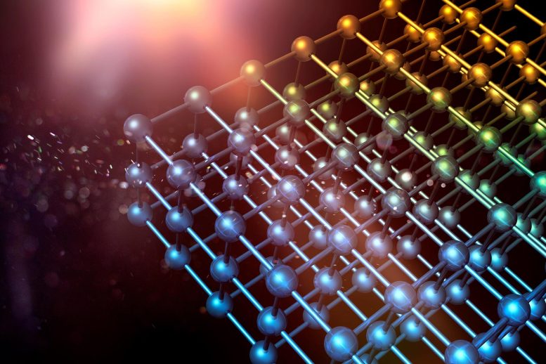
One-atom-thick materials generally take the form of a lattice, or a layer of geometrically aligned atoms that form a pattern specific to each material. A superlattice is made up of lattices of different materials stacked upon one another. Superlattices have completely new optical, chemical and physical properties which make them adaptable for specific applications such as photo optics and other sensors.
Breakthrough in Superlattice Manufacturing
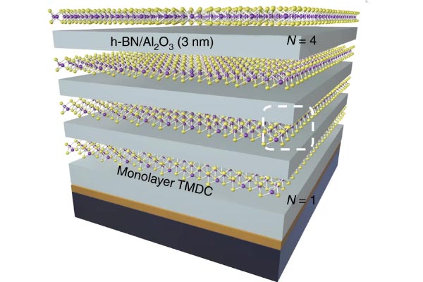
The team at Penn Engineering made a superlattice, five atoms thick, of tungsten and sulfur (WS2).
“After two years of research using simulations that informed us how the superlattice would interact with the environment, we were ready to experimentally build the superlattice,” says Kumar. “Because traditional superlattices are grown on a desired substrate directly, they tend to be millions of atoms thick, and difficult to transfer to other material substrates. We collaborated with industry partners to ensure that our atomically thin superlattices were grown to be scalable and applicable to many different materials.”
They grew monolayers of atoms, or lattices, on a two-inch wafer and then dissolved the substrate, which allows the lattice to be transferred to any desired material, in their case, sapphire. Additionally, their lattice was created with repeating units of atoms aligned in one direction to make the superlattice two-dimensional, compact, and efficient.
“Our design is scalable as well,” says Lynch. “We were able to create a superlattice with a surface area measured in centimeters with our method, which is a major improvement compared to the micron scale of silicon superlattices currently being produced. This scalability is possible due to the uniform thickness in our superlattices, which makes the manufacturing process simple and repeatable. Scalability is important to be able to place our superlattices on the industry-standard, four-inch chips.”
Advantages of the New Superlattice Design
Their superlattice design is not only extremely thin, making it lightweight and cost-effective, it can also emit light, not just detect it.
“We are using a new type of structure in our superlattices that involves exciton-polaritons, which are quasi-state particles made of half matter and half-light,” says Lynch. “Light is very hard to control, but we can control matter, and we found that by manipulating the shape of the superlattice, we could indirectly control light emitted from it. This means our superlattice can be a light source. This technology has the potential to significantly improve lidar systems in self-driving cars, facial recognition, and computer vision.”
Being able to both emit and detect light with the same material opens the door for more complicated applications.
“One current technology that I can see our superlattice being used for is in integrated photonic computer chips which are powered by light,” says Lynch. “Light moves faster than electrons, so a chip powered by light will increase computing speed, making the process more efficient, but the challenge has been finding a light source that can power the chip. Our superlattice may be a solution there.”
Potential Applications and Future Prospects
Applications for this new technology are diverse and will likely include high-tech robotics, rockets, and lasers. Because of the wide range of applications for these superlattices, the scalability is very important.
“Our superlattices are made with a general, non-sophisticated process that does not require multiple steps in a clean room, allowing the process to be repeated easily,” says Kumar. “Additionally, the design is applicable to many different types of materials, allowing for adaptability.”
“In the tech world, there is a constant evolution of things moving toward the nanoscale,” he says. “We will definitely be seeing a thinning down of microchips and the structures that make them, and our work in the two-dimensional material is part of this evolution.”
“Of course, as we thin things down and make technology smaller and smaller, we start to interact with quantum mechanics and that’s when we see interesting and unexpected phenomena occur,” says Lynch. “I am very excited to be a part of a team bringing quantum mechanics into high-impact technology.”
Reference: “Light–matter coupling in large-area van der Waals superlattices” by Pawan Kumar, Jason Lynch, Baokun Song, Haonan Ling, Francisco Barrera, Kim Kisslinger, Huiqin Zhang, Surendra B. Anantharaman, Jagrit Digani, Haoyue Zhu, Tanushree H. Choudhury, Clifford McAleese, Xiaochen Wang, Ben R. Conran, Oliver Whear, Michael J. Motala, Michael Snure, Christopher Muratore, Joan M. Redwing, Nicholas R. Glavin, Eric A. Stach, Artur R. Davoyan and Deep Jariwala, 2 December 2021, Nature Nanotechnology.
DOI: 10.1038/s41565-021-01023-x
Never miss a breakthrough: Join the SciTechDaily newsletter.
Follow us on Google and Google News.