Tiny crystal “seeds” could solve a hidden flaw in perovskite solar cells—unlocking high efficiency at larger scales.
Traditional perovskite solar cells (PSCs) are built with the electron transport layer underneath the perovskite light-absorbing layer and the hole transport layer on top. While this design has delivered strong performance in laboratories, it faces challenges when scaled up for mass production and long-term stability.
Inverted PSCs flip that structure, placing the hole-transport layer beneath the perovskite and the electron-transport layer above it. This configuration offers strong power conversion potential and works well with scalable solution-based manufacturing methods, making it an attractive option for next-generation solar technology.
However, inverted PSCs have struggled with a persistent weakness. Their efficiency and durability are often limited by microscopic structural irregularities and electronic defects at the bottom interface, also known as the buried interface, where the perovskite layer meets the hole transport layer. Because this region is hidden within the device, it has been especially difficult to control with precision.
Crystal-Solvate Pre-Seeding Strategy
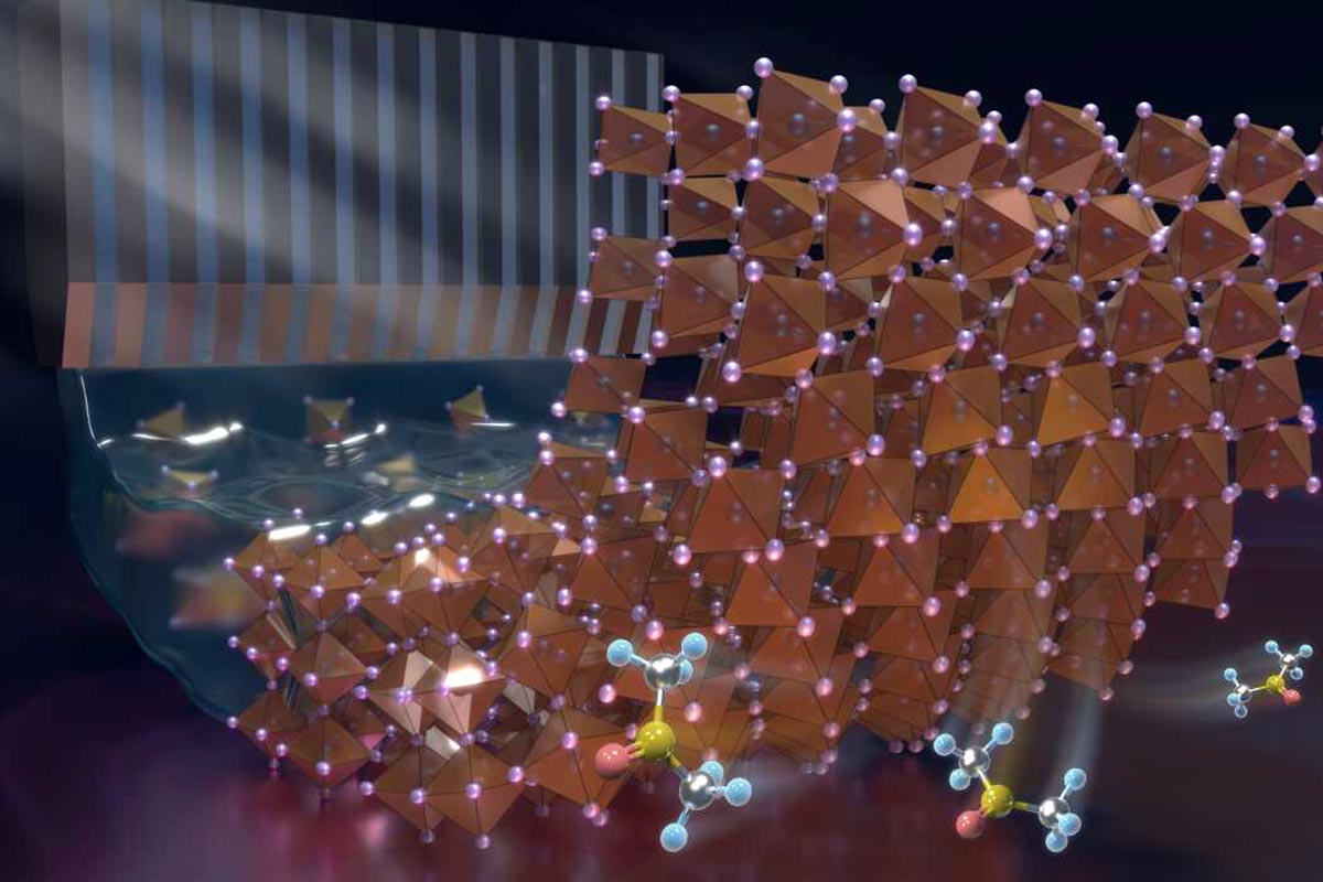
To tackle this issue, researchers at the Qingdao Institute of Bioenergy and Bioprocess Technology (QIBEBT) of the Chinese Academy of Sciences developed a crystal-solvate (CSV) pre-seeding approach designed to carefully manage this critical bottom interface. Their method opens the door to producing high-efficiency, large-area perovskite solar modules. The findings were published today (February 27) in Nature Synthesis.
The technique begins by depositing specially engineered low-dimensional halide crystal-solvate seeds with the chemical formula PDPbI4·DMSO onto self-assembled monolayer (SAM)-modified substrates. These CSV nanocrystals act as a structural guide for the perovskite layer that forms afterward.
The rod-shaped CSV nanocrystals improve how well the perovskite precursor solution spreads across the typically water-repelling SAM surface. This ensures even coverage. As the perovskite crystals begin to form, the pre-seeded nanocrystals serve as plentiful nucleation sites, helping the crystals grow more quickly and in a more organized way.
Lattice-Confined Solvent Annealing
A key feature of the method involves dimethyl sulfoxide (DMSO) molecules that are built into the CSV crystal structure. When the material is heated during thermal annealing, these DMSO molecules are gradually released. This creates what the team describes as a “lattice-confined solvent annealing” environment at the bottom interface.
This gentle, localized solvent atmosphere allows crystal grains to reorganize and grow more effectively. Combined with the guiding effect of the seeds, this process produces a more uniform and stable perovskite layer.
“We have developed an integrated approach that simultaneously addresses crystallization regulation and interface stabilization,” said Dr. Xiuhong Sun, co-first author of the study. “This strategy delivers good performance even at buried interfaces, which are notoriously challenging to precisely control.”
Improved Stability and Large-Area Performance
The result is a perovskite film with fewer voids at the interface and smoother grain boundaries. The bottom portion of the film (the perovskite “bottom layer”) becomes denser and more highly aligned, leading to improved electronic behavior and stronger resistance to heat and light-related stress.
The team also combined the CSV pre-seeding method with a slot-die coating process to produce a perovskite solar mini-module with an aperture area of 49.91 cm². The device achieved a power conversion efficiency of 23.15%. Notably, the drop in efficiency from small laboratory cells to the larger mini-module was less than 3%, a result that surpasses many earlier reports.
“This technology overcomes the longstanding scaling bottleneck caused by size effects through the combination of induced crystallization and buried interface restoration,” said Prof. Shuping Pang. “Beyond its direct application in perovskite photovoltaics, the crystal-solvate pre-seeding concept establishes a versatile material platform: By tuning organic cations and solvent molecules, a diverse library of CSV materials can be designed, opening up a new paradigm for interface engineering in perovskite photovoltaics and other soft-lattice semiconductor optoelectronic devices alike.”
Reference: “Crystal-solvate pre-seeded synthesis for scalable perovskite solar cell fabrication” by Xiuhong Sun, Mingwei Hao, Kaiyu Wang, Kuan Wang, Yalan Zhang, Bingqian Zhang, Xuexuan Huang, Chenghao Bi, Shuping Pang and Yuanyuan Zhou, 27 February 2026, Nature Synthesis.
DOI: 10.1038/s44160-026-00993-x
Never miss a breakthrough: Join the SciTechDaily newsletter.
Follow us on Google and Google News.
2 Comments
When does more Western scientists, start catching up to the many Chinese solar discoveries , particularly in Peroskite Solar cells ?
Seems many Peroskite solar advances , are coming from Chinese labs ? How many Western/Australian solar labs , are finding breakthroughs, with tbe promising ultra cheap Peroskite solar panels ?
Appears the promise of ultra cheap Peroskite solar cells….has slowed down in last few years ?
Will Ai breakthru….the current lack of long lasting Peroskite solar cells ?
AI won’t help, because AI as currently implemented does not conduct original research. Breakthroughs always come either from human thought, or accidental observations.