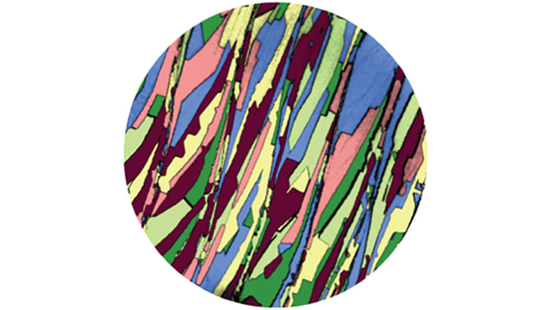
Each color in this figure represents a possible orientation of borophene crystals with respect to the surface of the Cu substrate. There are six possible orientations of these domains. Credit: Rongting Wu
The thinnest flake, just one atom thick, has provided scientists at Yale and the Brookhaven National Laboratory with new insight into a promising material for the next generation of high-speed electronics and a host of practical applications.
Sheets of boron, or borophene — a close cousin of graphene, a material 200 times stronger than steel that promised to revolutionize electronics — were first theorized in the mid-1990s, but synthesizing the material has defied scientists for almost a decade.
These composite materials, atomically thin with the greatest surface-to-mass ratios, are valuable for solar cells and energy storage, and are also accelerating the development of the fastest and smallest transistors, new touch screens, batteries, and water filters.
The challenge has been how to turn these naturally abundant elements into technologically useful materials.
While the potential electronic and elastic properties of two-dimensional (2D) boron crystals have excited the interest of scientists in the field, recent production of borophene flakes were too small for device fabrication, their “tunable” structure remaining unproven.
In a study published December 3 in Nature Nanotechnology, scientists at Yale’s Energy Sciences Institute have taken the next step in modifying the crystal structure of borophene by growing large, device-size crystals up to 100 square micrometers in size on copper surfaces.
“For most other known materials their structure is set. They are either impossible or very hard to morph from one stable structure into the other, rather like turning natural graphite into a diamond, even though they are both forms of carbon,” said Yale research scientist Adrian Gozar, the study’s senior author. “Borophene has exceptional properties that we can now think about stabilizing for literally numerous applications.”
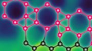
Theoretical calculations by graduate student Stephen Eltinge and professor of applied physics Sohrab Ismail-Beigi indicate a crystal structure consisting of a novel triangular network and an interaction between borophene and copper that is characterized by electronic charge transfer. Eltinge and Ismail-Beigi are co-authors of the new study.
With the new material’s potential to outmatch graphene in its elasticity, strength, and conductivity, the work has set the stage for fabricating borophene-based devices and brings closer the idea of borophene as a model for artificial 2D materials development, said the scientists.
Reference: “Large-area single-crystal sheets of borophene on Cu(111) surfaces” by Rongting Wu, Ilya K. Drozdov, Stephen Eltinge, Percy Zahl, Sohrab Ismail-Beigi, Ivan Božović and Adrian Gozar, 3 December 2018, Nature Nanotechnology.
DOI: 10.1038/s41565-018-0317-6
The study’s other authors are Yale’s Rongting Wu, Stephen Eltinge and Sohrab Ismail-Beigi, and Ivan Božović, Ilya K. Drozdov, and Percy Zahl of the Brookhaven National Laboratory.


Be the first to comment on "Borophene Breakthrough Provides New Insight Into a Promising Material"