Close Menu
    Facebook X (Twitter) Instagram
    SciTechDaily
    • Biology
    • Chemistry
    • Earth
    • Health
    • Physics
    • Science
    • Space
    • Technology
    Facebook X (Twitter) Pinterest YouTube RSS
    SciTechDaily
    Home»Technology»Laser Holograms Could Revolutionize 3D Chip Manufacturing
    Technology

    Laser Holograms Could Revolutionize 3D Chip Manufacturing

    By Julia Westbrook, University of Massachusetts AmherstApril 11, 2025No Comments5 Mins Read
    Facebook Twitter Pinterest Telegram LinkedIn WhatsApp Email Reddit
    Share
    Facebook Twitter LinkedIn Pinterest Telegram Email Reddit
    Semiconductors CPU Computer Chip Illustration
    Researchers at UMass Amherst developed a novel method for aligning 3D semiconductor chips using laser light and concentric metalenses, projecting holograms that reveal even atomic-scale misalignments. This breakthrough could reduce chip manufacturing costs, enable advanced 3D electronics, and lead to compact, affordable sensors.

    The approach uses lasers and holograms to detect misalignments as small as 0.017 nanometers.

    Researchers at the University of Massachusetts Amherst have developed a new method for aligning 3D semiconductor chips by shining a laser through concentric metalenses patterned onto the chips, creating a hologram. Their work, published in Nature Communications, could significantly reduce the cost of manufacturing 2D chips, support the development of 3D photonic and electronic chips, and open the door to affordable, compact sensor technologies.

    Semiconductor chips power electronic devices by enabling them to process, store, and transmit information. These functions rely on precise patterns of components embedded in the chip. However, the traditional 2D chip design has reached the limits of its technological potential, and 3D integration is now seen as the most promising path forward.

    Simulated and Measured Results of Different Sizes of Lateral Misalignment
    Simulated and measured results of different sizes of lateral misalignment, from 150 nm to 1 micrometer (or 1,000 nm). Credit: Amir Arbabi

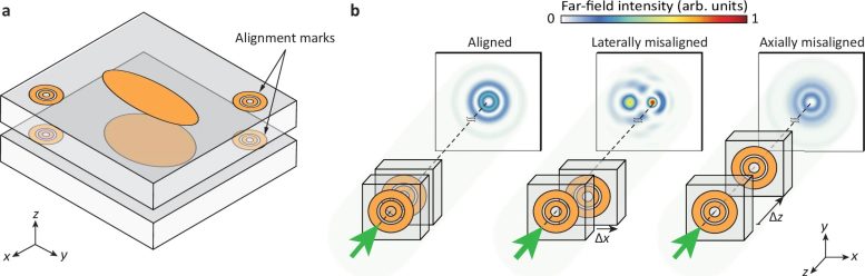
    To build a 3D chip, several 2D chips are stacked together. Their layers must be aligned with extreme precision, down to tens of nanometers. This alignment must occur across all three dimensions: front to back, side to side, and the vertical distance between layers (known as the x, y, and z axes).

    Limitations of traditional alignment

    “The traditional approach for aligning two layers is to look with a microscope for marks (typically corners or crosshairs) on the two layers and to try to overlap them,” explains Amir Arbabi, associate professor of electrical and computer engineering at UMass Amherst and senior author on the paper.

    Holographic Feedback Reveals Chip Alignment Precision
    [Left] Semiconductor layers are stacked using concentric metalenses as alignment marks. [Right] Light shines through these marks to project a hologram. The alignment or misalignment of the lenses dictates the hologram’s appearance. Credit: Amir Arbabi
    Existing microscope-based alignment methods are ill-suited for making these 3D chips.

    “The microscope cannot simultaneously see both crosshairs in focus because the gap between the layers is hundreds of microns, and the motion to refocus between layers introduces opportunities for the chips to shift and further misalign.” says Maryam Ghahremani, doctoral candidate and lead author on the paper. Also “the smallest features you can resolve are set by the diffraction limit, which is around 200 nanometers,” she adds.

    Simulated and Measured Results of Different Sizes of Misalignment in the Gap Between Two Layers
    Simulated and measured results of different sizes of misalignment in the gap between two layers, from 1 micrometer (or 1,000 nm) to 3 µm. Credit: Amir Arbabi

    Breakthrough in nanometer-scale detection

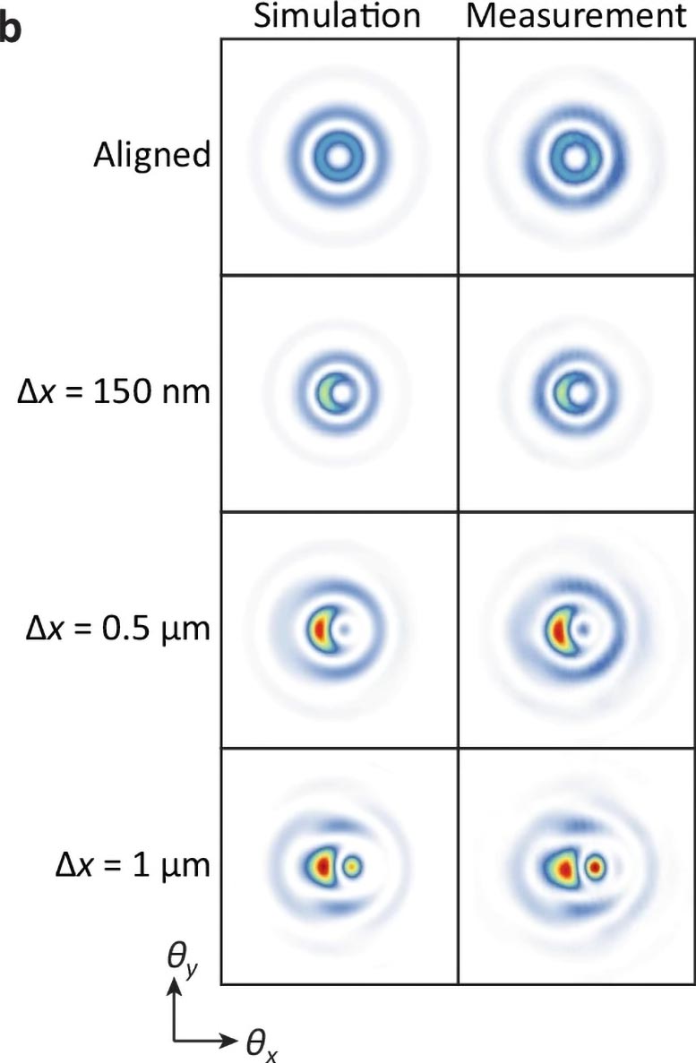
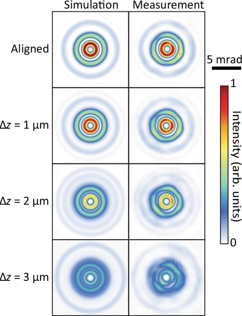
    The new alignment method created by Arbabi and his team has no moving parts and can see misalignments between two distant layers at a much smaller scale. The researchers were hoping to reach 100-nm precision. Instead, their method finds errors up to 0.017 nm along side-to-side measures (x and y axes) and 0.134 nm when assessing the distance between the two chips (z-axis).

    “Consider you have two objects. By looking at the light that goes through them, we can see if one moved by the size of an atom with respect to the other one,” Arbabi says, far exceeding their expectations. The naked eye can spot errors as small as a few nanometers, and computers can read even smaller ones.

    Visualizing Nanometer Scale Misalignment With Holographic Intensity Patterns
    Computers can read misalignments undetectable by the naked eye, as illustrated by this 10-nm lateral misalignment. Credit: Amir Arbabi

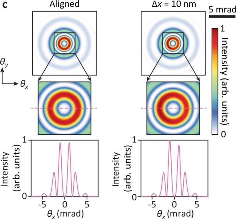
    To achieve this, they embedded alignment marks made from concentric metalenses on the semiconductor chip. When light from a laser shines through these marks on both chips, it projects two interfering holograms. “This interference image shows if the chips are aligned or not, as well as the direction and the amount of their misalignment,” says Ghahremani.

    “[Chip alignment] is a big, costly challenge for some of the companies that work in manufacturing semiconductor tools,” Arbabi says. “Our approach addresses one of the challenges of making them.” Lower costs also increase access to this technology for smaller startup companies looking to innovate with semiconductors.

    Arbabi also points out that this method can be used to make displacement sensors that can be used for measuring displacements and other quantities. “Many physical quantities that you want to detect can be translated to displacements, and the only thing you need is a simple laser and a camera,” he says. For instance, “if you want a pressure sensor, you could measure the movement of a membrane.” Anything that involves movement —vibration, heat, acceleration — can in theory be tracked by this method.

    Reference: “3D alignment of distant patterns with deep-subwavelength precision using metasurfaces” by Maryam Ghahremani, Andrew McClung, Babak Mirzapourbeinekalaye and Amir Arbabi, 14 October 2024, Nature Communications.
    DOI: 10.1038/s41467-024-53219-z

    Funding: U.S. National Science Foundation

    Never miss a breakthrough: Join the SciTechDaily newsletter.
    Follow us on Google and Google News.

    Optoelectronics Photonics Semiconductors University of Massachusetts Amherst
    Share. Facebook Twitter Pinterest LinkedIn Email Reddit

    Related Articles

    Scientists Discover “Shape-Shifting” Semiconductors Activated by Light

    How “Empty Space” Is Supercharging Atomically Thin Semiconductors

    Breaking the Bottleneck: All-Optical Chip Could Unlock Light-Speed Communication

    Revolutionizing Photonics: Lithium Tantalate Powers Next-Gen Optical Circuits

    Superconducting Silicon-Photonic Chip Developed for Quantum Communication

    A Laser Breakthrough: First Commercially Scalable Integrated Laser and Microcomb on a Single Chip

    Breakthrough in the Creation of Electrically Driven Nanolasers for Integrated Circuits

    Revolutionary Light-Emitting Silicon – “Holy Grail” Breakthrough After 50 Years of Work

    Light-Emitting Diode and Photodetector for Silicon CMOS Chips

    Leave A Reply Cancel Reply

    • Facebook
    • Twitter
    • Pinterest
    • YouTube

    Don't Miss a Discovery

    Subscribe for the Latest in Science & Tech!

    Trending News

    Your Blood Pressure Reading Could Be Wrong Because of One Simple Mistake

    Astronomers Stunned by Ancient Galaxy With No Spin

    Physicists May Be on the Verge of Discovering “New Physics” at CERN

    Scientists Solve 320-Million-Year Mystery of Reptile Skin Armor

    Scientists Say This Daily Walking Habit May Be the Secret to Keeping Weight Off After Dieting

    New Therapy Rewires the Brain To Restore Joy in Depression Patients

    Giant Squid Detected off Western Australia in Stunning Deep-Sea Discovery

    Popular Sugar-Free Sweetener Linked to Liver Disease, Study Warns

    Follow SciTechDaily
    • Facebook
    • Twitter
    • YouTube
    • Pinterest
    • Newsletter
    • RSS
    SciTech News
    • Biology News
    • Chemistry News
    • Earth News
    • Health News
    • Physics News
    • Science News
    • Space News
    • Technology News
    Recent Posts
    • New Stroke Study Challenges Decades-Old Medical Beliefs
    • These Simple Plant Foods Are Linked to Lower Blood Pressure
    • Common Blood Pressure Drug Supercharges Cancer Treatment in Surprising New Study
    • Key Magic Mushroom Ingredient Increases Laziness and Reduces Aggression
    • Researchers Solve 15-Year Mystery Behind Cancer-Causing Gut Toxin
    Copyright © 1998 - 2026 SciTechDaily. All Rights Reserved.
    • Science News
    • About
    • Contact
    • Editorial Board
    • Privacy Policy
    • Terms of Use

    Type above and press Enter to search. Press Esc to cancel.