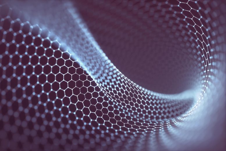
Understanding how electrons move in 2-D layered material systems could lead to advances in quantum computing and communication.
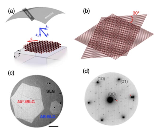
Scientists studying two different configurations of bilayer graphene—the two-dimensional (2-D), atom-thin form of carbon—have detected electronic and optical interlayer resonances. In these resonant states, electrons bounce back and forth between the two atomic planes in the 2-D interface at the same frequency. By characterizing these states, they found that twisting one of the graphene layers by 30 degrees relative to the other, instead of stacking the layers directly on top of each other, shifts the resonance to a lower energy.
From this result, just published in Physical Review Letters, they deduced that the distance between the two layers increased significantly in the twisted configuration, compared to the stacked one. When this distance changes, so do the interlayer interactions, influencing how electrons move in the bilayer system. An understanding of this electron motion could inform the design of future quantum technologies for more powerful computing and more secure communication.
“Today’s computer chips are based on our knowledge of how electrons move in semiconductors, specifically silicon,” said first and co-corresponding author Zhongwei Dai, a postdoc in the Interface Science and Catalysis Group at the Center for Functional Nanomaterials (CFN) at the U.S. Department of Energy (DOE)’s Brookhaven National Laboratory. “But the physical properties of silicon are reaching a physical limit in terms of how small transistors can be made and how many can fit on a chip. If we can understand how electrons move at the small scale of a few nanometers in the reduced dimensions of 2-D materials, we may be able to unlock another way to utilize electrons for quantum information science.”
Quantum Confinement Effects at the Nanoscale
At a few nanometers, or billionths of a meter, the size of a material system is comparable to that of the wavelength of electrons. When electrons are confined in a space with dimensions of their wavelength, the material’s electronic and optical properties change. These quantum confinement effects are the result of quantum mechanical wave-like motion rather than classical mechanical motion, in which electrons move through a material and are scattered by random defects.
Custom Substrates Enable Dual Characterization
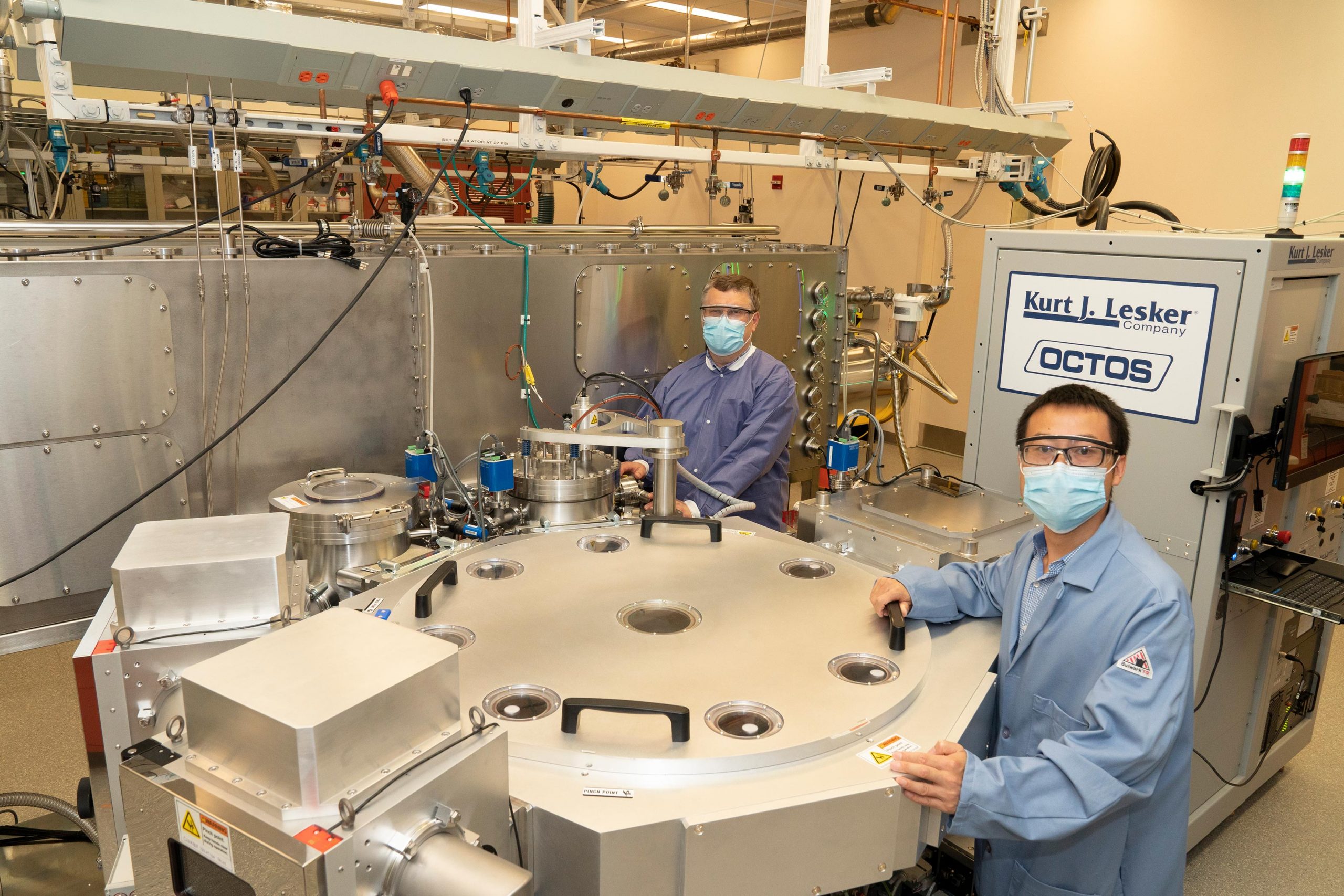
For this research, the team selected a simple material model—graphene—to investigate quantum confinement effects, applying two different probes: electrons and photons (particles of light). To probe both electronic and optical resonances, they used a special substrate onto which the graphene could be transferred. Co-corresponding author and CFN Interface Science and Catalysis Group scientist Jurek Sadowski had previously designed this substrate for the Quantum Material Press (QPress). The QPress is an automated tool under development in the CFN Materials Synthesis and Characterization Facility for the synthesis, processing, and characterization of layered 2-D materials. Conventionally, scientists exfoliate 2-D material “flakes” from 3-D parent crystals (e.g., graphene from graphite) on a silicon dioxide substrate several hundred nanometers thick. However, this substrate is insulating, and thus electron-based interrogation techniques don’t work. So, Sadowski and CFN scientist Chang-Yong Nam and Stony Brook University graduate student Ashwanth Subramanian deposited a conductive layer of titanium oxide only three nanometers thick on the silicon dioxide substrate.
“This layer is transparent enough for optical characterization and determination of the thickness of exfoliated flakes and stacked monolayers while conductive enough for electron microscopy or synchrotron-based spectroscopy techniques,” explained Sadowski.
In the Charlie Johnson Group at the University of Pennsylvania—Rebecca W. Bushnell Professor of Physics and Astronomy Charlie Johnson, postdoc Qicheng Zhang, and former postdoc Zhaoli Gao (now an assistant professor at the Chinese University of Hong Kong)—grew the graphene on metal foils and transferred it onto the titanium oxide/silicon dioxide substrate. When graphene is grown in this way, all three domains (single layer, stacked, and twisted) are present.
Then, Dai and Sadowski designed and carried out experiments in which they shot electrons into the material with a low-energy electron microscope (LEEM) and detected the reflected electrons. They also fired photons from a laser-based optical microscope with a spectrometer into the material and analyzed the spectrum of light scattered back. This confocal Raman microscope is part of the QPress cataloger, which together with image-analysis software, can pinpoint the locations of sample areas of interest.
“The QPress Raman microscope enabled us to quickly identify the target sample area, accelerating our research,” said Dai.
Their results suggested that the spacing between layers in the twisted graphene configuration increased by about six percent relative to the non-twisted configuration. Calculations by theorists at the University of New Hampshire verified the unique resonant electronic behavior in the twisted configuration.
“Devices made out of rotated graphene may have very interesting and unexpected properties because of the increased interlayer spacing in which electrons can move,” said Sadowski.
Next, the team will fabricate devices with the twisted graphene. The team will also build upon initial experiments conducted by CFN staff scientist Samuel Tenney and CFN postdocs Calley Eads and Nikhil Tiwale to explore how adding different materials to the layered structure impacts its electronic and optical properties.
Expanding the Toolkit for Quantum Information Science
“In this initial research, we picked the simplest 2-D material system we can synthesize and control to understand how electrons behave,” said Dai. “We plan to continue these types of fundamental studies, hopefully shedding light on how to manipulate materials for quantum computing and communications.”
This research was supported by the DOE Office of Science and used resources of the CFN and National Synchrotron Light Source II (NSLS-II), both DOE Office of Science User Facilities at Brookhaven. The LEEM microscope is part of the x-ray photoemission electron microscopy (XPEEM)/LEEM endstation of the Electron Spectro-Microscopy beamline at NSLS-II; the CFN operates this endstation through a partner user agreement with NSLS-II. The other funding agencies are the National Science Foundation, Research Grant Council of Hong Kong Special Administrative Region, and the Chinese University of Hong Kong.
For more on this research, read Atomically-Thin, Twisted Graphene Has Unique Properties That Could Advance Quantum Computing.
Reference: “Quantum-Well Bound States in Graphene Heterostructure Interfaces” by Zhongwei Dai, Zhaoli Gao, Sergey S. Pershoguba, Nikhil Tiwale, Ashwanth Subramanian, Qicheng Zhang, Calley Eads, Samuel A. Tenney, Richard M. Osgood, Chang-Yong Nam, Jiadong Zang, A. T. Charlie Johnson and Jerzy T. Sadowski, 20 August 2021, Physical Review Letters.
DOI: 10.1103/PhysRevLett.127.086805
Never miss a breakthrough: Join the SciTechDaily newsletter.
Follow us on Google and Google News.