Work on three graphene-based devices may yield new insights into superconductivity.
MIT researchers and colleagues have turned a “magic” material composed of atomically thin layers of carbon into three useful electronic devices. Normally, such devices, all key to the quantum electronics industry, are created using a variety of materials that require multiple fabrication steps. The MIT approach automatically solves a variety of problems associated with those more complicated processes.
As a result, the work could usher in a new generation of quantum electronic devices for applications including quantum computing. Further, the devices can be superconducting, or conduct electricity without resistance. They do so, however, through an unconventional mechanism that, with further study, could give new insights into the physics of superconductivity. The researchers reported their results in the May 3, 2021, issue of Nature Nanotechnology.
“In this work we have demonstrated that magic-angle graphene is the most versatile of all superconducting materials, allowing us to realize in a single system a multitude of quantum electronic devices. Using this advanced platform, we have been able to explore for the first time novel superconducting physics that only appears in two dimensions,” says Pablo Jarillo-Herrero, the Cecil and Ida Green Professor of Physics at MIT and leader of the work. Jarillo-Herrero is also affiliated with MIT’s Materials Research Laboratory.
A Mmagic Angle
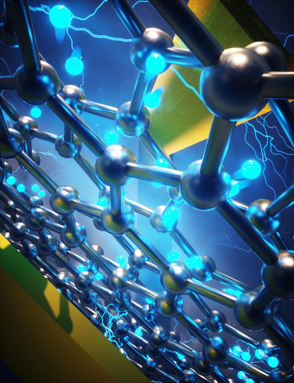
The new “magic” material is based on graphene, a single layer of carbon atoms arranged in hexagons resembling a honeycomb structure. Since the first unambiguous isolation of graphene in 2004, interest in this material has skyrocketed due to its unique properties. For example, it is stronger than diamond, transparent, and flexible. It also easily conducts both heat and electricity.
In 2018, the Jarillo-Herrero group made a startling discovery involving two layers of graphene, one placed on top of the other. Those layers, however, weren’t exactly on top of each other; rather, one was slightly rotated at a “magic angle” of 1.1 degrees.

The resulting structure allowed the graphene to be either a superconductor or an insulator (which prevents the flow of electrical current), depending on the number of electrons in the system as provided by an electric field. Essentially, the team was able to tune graphene into completely different states by changing the voltage at the turn of a knob.
The overall “magic” material, formally known as magic-angle twisted bilayer graphene (MATBG), has generated intense interest in the research community, even inspiring a new field known as twistronics. It is also at the heart of the current work.
In 2018, Jarillo-Herrero and coworkers changed the voltage supplied to the magic material via a single electrode, or metallic gate. In the current work, “we introduced multiple gates to subject different areas of the material to different electric fields,” says Daniel Rodan-Legrain, a graduate student in physics and lead author of the Nature Nanotechnology paper.
Suddenly, the team was able to tune different sections of the same magic material into a plethora of electronic states, from superconducting to insulating to somewhere in between. Then, by applying gates in different configurations, they were able to reproduce all of the parts of an electronic circuit that would ordinarily be created with completely different materials.
Working Devices
Ultimately, the team used this approach to create three different working quantum electronic devices. These devices include a Josephson junction, or superconducting switch. Josephson junctions are the building blocks of the quantum bits, or qubits, behind superconducting quantum computers. They also have a variety of other applications, such as incorporation into devices that can make very precise measurements of magnetic fields.
The team also created two related devices: a spectroscopic tunneling device and a single-electron transistor, or a very sensitive device for controlling the movement of electricity, literally one electron at a time. The former is key to studying superconductivity, while the latter has a variety of applications, in part because of its extreme sensitivity to electric fields.
All three devices benefit from being made of a single electrically tunable material. Those made conventionally, of multiple materials, suffer from a variety of challenges. For example, different materials may be incompatible. “Now, if you’re dealing with one single material, those problems disappear,” says Rodan-Legrain.
William Oliver, an MIT associate professor in the Department of Electrical Engineering and Computer Science who was not involved in the research, says: “MATBG has the remarkable property that its electrical properties — metallic, superconducting, insulating, etc. — can be determined by applying a voltage to a nearby gate. In this work, Rodan-Legrain et al. have shown that they can make rather complicated devices comprising superconducting, normal, and insulating regions by electrical gating of a single flake of MATBG. The conventional approach would be to fabricate the device in several steps using different materials. With MATBG, the resulting devices are fully reconfigurable by simply changing the gate voltages.”
Toward the Future
The work described in the Nature Nanotechnology paper paves the way for many potential future advances. For example, says Rodan-Legrain, it could be used to create the first voltage-tunable qubit from a single material, which could be applied in future quantum computers.
In addition, because the new system enables more detailed studies of the enigmatic superconductivity in MATBG, and is relatively easy to work with, the team is hopeful that it could allow insights into the creation of high-temperature superconductors. Current superconductors can only operate at very low temperatures. “That is actually one of the big hopes [behind our magic material],” says Rodan-Legrain. “Can we use it as a kind of Rosetta Stone” to better understand its high-temperature cousins?
In a glimpse into how science works, Rodan-Legrain describes the surprises the team encountered while conducting the research. For example, some of the data from the experiments didn’t correspond to the team’s initial expectations. That’s because the Josephson junctions they created using atomically thin MATGB were two-dimensional, and thus had a notably different behavior from their 3D conventional counterparts. “It was great having the data come through, seeing them, being puzzled about them, and then further understanding and making sense of what we saw.”
Reference: “Highly tunable junctions and non-local Josephson effect in magic-angle graphene tunnelling devices” by Daniel Rodan-Legrain, Yuan Cao, Jeong Min Park, Sergio C. de la Barrera, Mallika T. Randeria, Kenji Watanabe, Takashi Taniguchi and Pablo Jarillo-Herrero, 3 May 2021, Nature Nanotechnology.
DOI: 10.1038/s41565-021-00894-4
In addition to Jarillo-Herrero and Rodan-Legrain, additional authors of the paper are Yuan Cao, a postdoc in MIT’s Materials Research Laboratory (MRL); Jeong Min Park, a graduate student in the Department of Chemistry; Sergio C. de la Barrera, a postdoc in the MRL; Mallika T. Randeria, a Pappalardo Postdoctoral Fellow in the Department of Physics; and Kenji Watanabe and Takashi Taniguchi, both of the National Institute for Materials Science in Japan. (Rodan-Legrain, Cao, and Park were equal contributors to the paper.)
This work was supported by the U.S. National Science Foundation, the U.S. Department of Energy, the U.S. Army Research Office, the Fundació Bancaria “la Caixa,” the Gordon and Betty Moore Foundation, the Fundación Ramon Areces, an MIT Pappalardo Fellowship, and the Ministry of Education, Culture, Sports, Science and Technology (MEXT) of Japan.
Never miss a breakthrough: Join the SciTechDaily newsletter.
Follow us on Google and Google News.
3 Comments
make these really cheaply, and you’ve got fantastic computation, and communication equipment. Many in parallel make the perfect power electronics “transistor”. Just think, used in digital equipment, off is a perfect insulator, on is superconductor, I’m not even sure how I’d define it’s forbidden region of voltage in the digital circuitry.
In analog it has an active region, where change in voltage of the gate results in change in currrent, could be it’s linear, as you would want.
Wonder how much material needed to protect from radiation/EMP, ie coming solar flare activity? Would it improve, with the MABXX, solar cell out puts, ion engine output, allow finer focusing in lazer apps? Lots of interesting doors to explore indeed.
The applied science of the same, will open doors to many uses, since information can travel, almost in real time.Therefore also researches made in different fields, with the products of the same and through simulation will require or can obtain, almost real time result.Therefore, obtain know how, of mysteries, we have never known about.