A new microscopy technique allows scientists to see single-atom-thick boron nitride by making it glow under infrared light.
Researchers from the Physical Chemistry and Theory departments at the Fritz Haber Institute have developed a new way to visualize boron nitride layers that are just one atom thick. These ultrathin sheets are typically almost impossible to detect with standard optical microscopes because they lack optical resonances, making them effectively transparent.
To overcome this limitation, the team uses nonlinear microscopy with infrared light so that monolayers of hexagonal boron nitride (hBN) light up brightly. Their sum-frequency microscopy approach resonantly drives a lattice vibration in hBN, producing a strong signal that not only makes the material visible but also reveals its crystal orientation. This capability is significant for the large and thriving field of two-dimensional (2D) materials research and could support the development of new (opto-)electronic devices built by stacking 2D layers.
Why study 2D materials?
2D materials are crystalline substances made from a single layer of atoms, and their extreme thinness can produce unusual and useful properties. Although scientists have known about layered materials for more than a century, it was not until 2004 that the first isolated 2D layer, namely graphene, was successfully produced.
Since that breakthrough, researchers have created many more 2D materials and uncovered a growing range of potential uses. Because these atom-thin layers are promising for future technologies, including electronics, energy systems, and optical components, they remain a major focus of materials science research.
The challenge with hexagonal boron nitride
Boron nitride (BN) – also known as “white graphene” – is a layered material composed of the elements boron (B) and nitrogen (N), and can exist in various forms, including hexagonal boron nitride (hBN). Similar to graphene, hBN has a hexagonal lattice structure and its 2D layers are widely used in various applications, such as quantum optics or infrared nanophotonics, or simply as a substrate or encapsulating material.
For such applications, a precise characterization of the h-BN layers is critical. However, aside from the pronounced mid-infrared resonance, as a monolayer, hBN is transparent across the entire near-IR and visible spectral range. Thus, it cannot be studied using conventional optical microscopes.
This restriction has so far hindered its use in the development of new materials. For example, to identify possible distortions and grain boundaries in 2D layers, they must be accurately mapped.
Moreover, researchers stack monolayers of 2D materials on top of each other to create “van der Waals structures” that can exhibit completely new and exciting properties. Ideally, this layering could be screened live under a microscope and the orientation of the individual layers visualized. The development of such capabilities for hBN are hence highly desired.
The sum-frequency microscope
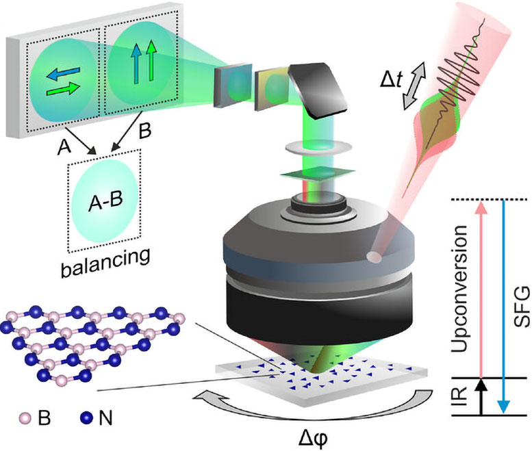
The research team at the Fritz Haber Institute overcame this challenge through their recently developed microscope that uses a trick in nonlinear optics to make the otherwise invisible material hBN visible. Their method, called “phase-resolved sum-frequency microscopy,” mixes two laser beams, one in the mid-infrared and one in the visible range, to generate a sum-frequency signal in the sample that is measured.
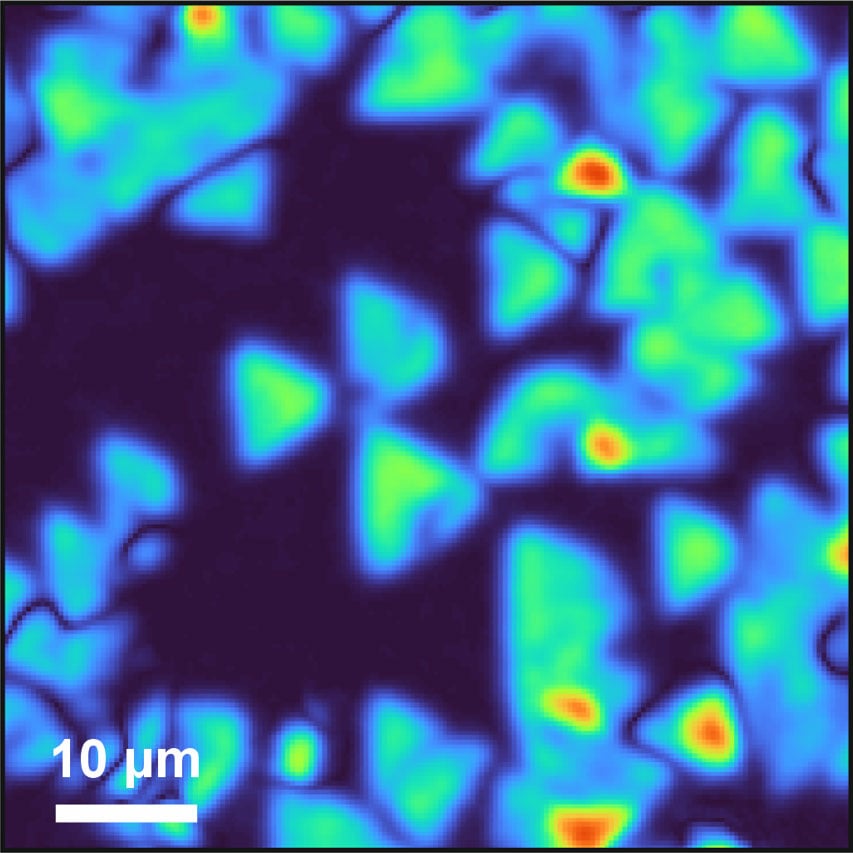
By resonantly driving an hBN lattice vibration, the measured sum-frequency signal becomes very intense, making it not only possible to image large 100 × 100 μm2 sample areas in less than 1 s, but also even visualize the crystal orientation.
Thanks to their new microscope, the researchers revealed that the 2D layers of hBN that grow in triangular domains display nitrogen-terminated zigzag edges. Moreover, the observed high nonlinearity in the frequency range of the vibrational resonance highlights monolayer hBN as a promising material for frequency upconversion – from the infrared into the visible – in new optoelectronic devices.
Fruitful cooperation of two FHI Departments and international partners
This study is a testament to the highly collaborative research philosophy of the Fritz Haber Institute combining the expertise of multiple research groups from its different departments as well as its many international partners in joint projects to tackle major challenges in science.
The hBN monolayer samples were synthesized at Vanderbilt University and then analyzed by sum-frequency microscopy at the Physical Chemistry Department at the Fritz Haber Institute.
To support the advanced characterization of the samples, atomic force microscopy (AFM) images were recorded by collaboration partners in the Department of Physics at the Freie Universitat Berlin. Finally, incorporating the expertise of the Theory Department at the Fritz Haber Institute enabled the crystallographic details to be extracted.
Prospects of the new experimental method
The newly developed microscope offers clear advantages over other existing methods. First and foremost, it can make optically transparent materials visible in an optical microscope. The resulting images have much higher contrast than traditional AFM images, and the use of the vibrational resonance enhancement enables “live imaging” of hBN, including online information on its crystal orientation.
These advanced capabilities make a controlled fabrication of layered van der Waals structures feasible in future applications. Finally, the authors also anticipate an extension of this new imaging tool as a non-invasive and label-free method to study a wider range of stacked 2D-materials, as well as their combinations with anisotropic molecular assemblies.
Reference: “Full Crystallographic Imaging of Hexagonal Boron Nitride Monolayers with Phonon-Enhanced Sum-Frequency Microscopy” by Niclas S. Mueller, Alexander P. Fellows, Ben John, Andrew E. Naclerio, Christian Carbogno, Katayoun Gharagozloo-Hubmann, Damián Baláž, Ryan A. Kowalski, Hendrik H. Heenen, Christoph Scheurer, Karsten Reuter, Joshua D. Caldwell, Martin Wolf, Piran R. Kidambi, Martin Thämer and Alexander Paarmann, 20 November 2025, Advanced Materials.
DOI: 10.1002/adma.202510124
Funding: Deutsche Forschungsgemeinschaft, European Commission
Never miss a breakthrough: Join the SciTechDaily newsletter.
Follow us on Google and Google News.