Using a technique called “patterned regrowth,” scientists at Cornell have invented a way to pattern single atom films of graphene and boron nitride without the use of a silicon substrate, an important step towards developing atomically thin integrated circuitry.
Integrated circuits, which are in everything from coffeemakers to computers and are patterned from perfectly crystalline silicon, are quite thin — but Cornell researchers think they can push thin-film boundaries to the single-atom level.
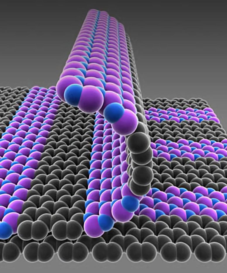
Their materials of choice are graphene, single-atom-thick sheets of repeating carbon atoms, and hexagonal boron nitride, similarly thin sheets of repeating boron and nitrogen atoms. Researchers led by Jiwoong Park, assistant professor of chemistry and chemical biology, have invented a way to pattern single-atom films of graphene and boron nitride, an insulator, without the use of a silicon substrate. The work is detailed in an article in the journal Nature, published online on August 30.
The technique, which they call patterned regrowth, could lead to substrate-free, atomically thin circuits — so thin, they could float on water or through air, but with tensile strength and top-notch electrical performance.
“We know how to grow graphene in single-atom-thick films, and we know how to grow boron nitride,” Park said. “But can we bring them together side and side? And when you bring them together, what happens at their junctions?”
As it turns out, researchers’ patterned regrowth, which harnesses the same basic photolithography technology used in silicon wafer processing, allows graphene and boron nitride to grow in perfectly flat, structurally smooth films — no creases or bumps, like a well-knitted scarf — which, if combined with the final, yet to be realized step of introducing a semiconductor material, could lead to the first atomically thin integrated circuit.
Simple really is beautiful, especially in the case of thin films, because photolithography is a well-established technique that forms the basis for making integrated circuits by laying materials, one layer at a time, on flat silicon.
Patterned regrowth is a bit like stenciling, Park said. He and colleagues first grew graphene on copper and used photolithography to expose graphene on selected areas, depending on the desired pattern. They filled that exposed copper surface with boron nitride, the insulator, which grows on copper and “fills the gaps in very nicely.”
“In the end, it forms a very nice cloth you just peel off,” Park said.
The research team, which includes David A. Muller, professor of applied and engineering physics, is working to determine what material would best work with graphene-boron nitride thin films to make up the final semiconducting layer that could turn the films into actual devices.
The team was helped by already being skilled at making graphene — still relatively new in the materials world — as well as Muller’s expertise in electron microscopy characterization at the nanoscale. Muller helped the team confirm that the lateral junctions of the two materials were, indeed, smooth and well-connected.
Reference: “Graphene and boron nitride lateral heterostructures for atomically thin circuitry” by Mark P. Levendorf, Cheol-Joo Kim, Lola Brown, Pinshane Y. Huang, Robin W. Havener, David A. Muller and Jiwoong Park, 29 August 2012, Nature.
DOI: 10.1038/nature11408
The paper’s co-first authors were chemistry graduate student Mark Levendorf and postdoctoral associate Cheol-Joo Kim, who fabricated the graphene and boron nitride samples and also performed the patterned regrowth at the Cornell NanoScale Science and Technology Facility.
The work was supported primarily by the Air Force Office of Scientific Research, and the National Science Foundation through the Cornell Center for Materials Research.
Never miss a breakthrough: Join the SciTechDaily newsletter.
Follow us on Google and Google News.