A novel and better approach at detecting non-uniformities in the optical properties of two-dimensional materials could potentially open the door to new uses for these materials, such as for drug detection, according to a team of researchers.
“The Two-Dimensional Crystal Consortium (2DCC) is a world leader in 2D materials research and my lab often works with the 2DCC doing materials characterization for novel 2D materials,” said Slava V. Rotkin, Frontier Professor of Engineering Science and Mechanics with an appointment in the Materials Research Institute at Penn State. “There is a big challenge in these studies: Frequently, optical properties of 2D materials are not uniform in space. Furthermore, they may vary at a very small spatial scale, down to a single atom.”
Rotkin and other researchers were able to take one step toward a possible solution, which was outlined in ACS Nano. While Rotkin stresses they only gave a demonstration of the principle in the study, the solution they propose was used for van der Waals heterostructures which could enable sensors made with 2D materials, materials that are one to a few atoms thick.
Surface-to-Volume Ratio in 2D Sensors
Sensors can be developed that enable sensing of bio-, chemical, and/or medical analytes of interest. Analytes are specific chemicals targeted for measurement or analysis. A good sensor detects these analytes with minimal sample preparation, in an abbreviated time frame, with low detection limits, and using samples containing substances other than the key analyte.
Identifying and understanding the variability of properties in materials could be extremely important for applications of 2D materials as sensors. The sensor material typically can only interact with the analyte at the surface. Thus, the material’s surface is an active area, while material’s volume is not. The larger the ratio of surface to volume, the lower the fraction of material which cannot be used. Such atomically thin materials have the ultimate surface-to-volume ratio for sensor use and may possess surface non-uniformities at the nanometer scale. This includes atomic impurities, adsorbates, defects, wrinkles, ruptures, etc. Such features can modulate the optical properties.
“Despite this being critical for effectiveness in certain application of 2D materials, there is currently no truly effective approach to detect these variabilities,” Rotkin said. “Due to their being so tiny, they are undetectable by optical tools and non-optical tools cannot resolve optical contrast.”
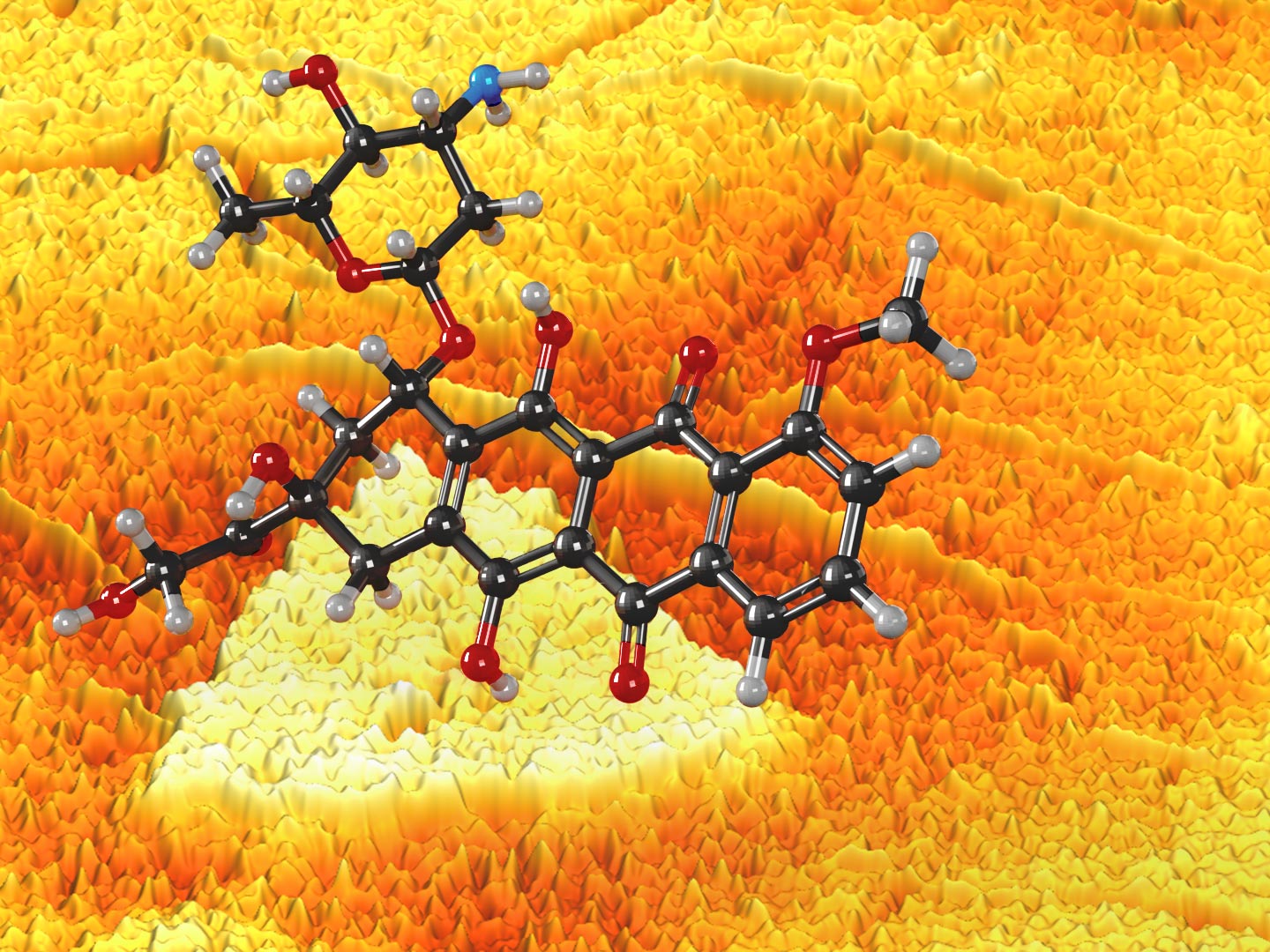
The researchers conducted experiments using a heterostructure material made of graphene, the 2D material version of graphite, and the inorganic compound molybdenum disulfide. The molybdenum disulfide gives a photoluminescence signal that detects the amount of charge transfer between the graphene and the molybdenum disulfide layers. Therefore, it can detect changes due to the bio analyte, which in this case is the cancer treatment drug doxorubicin, that can affect the charge.
These changes are also detectable in graphene via analysis by Raman spectroscopy, which discovers unique vibrations in molecules. A Raman microscope picks up shifts in the frequency of photons in the laser light beam caused by these vibrations.
“The two channels together allow a better calibration of the two signals against analyte concentration and the type of analyte,” Rotkin said. “And additionally, graphene enhances the Raman signal of the analyte itself to the extent one can ‘see’ a signal from just a few molecules.”
Label-Free Biosensing for Cancer Drug Detection
The researchers used doxorubicin as their analyte because it is a common cancer drug used in chemotherapy, and there is an acute need for biosensors to detect it to help regulate dosage and reduce side effects. There are two types of biosensors that work for this purpose, label-free biosensors, which can be used to detect a variety of drugs, and label-based biosensors, which can detect only a specific drug. The researchers used label-free biosensing in the study.
“The label-based biosensor is like a lock that can be opened with only one key, but the label-free biosensor is like a lock with many different keys,” Rotkin said. “We did not invent label-free multimodal biosensing, this approach has been in other studies. But an actual demonstration with a specific material is new and still important by itself.”
This could lead to steps for solving various health care challenges.
“Keeping in mind that there is a gap between fundamental research and its applications, I would say we contributed a brick to building a large set of nanotechnology/nanomaterials for biosensing and other applications,” Rotkin said. “Label-free detection lays the groundwork for smart and integrated sensors, new bio-threat safety techniques, and more individualized medicine and treatments, among others benefits.”
This is also significant because creating a label-free biosensor is more challenging than developing a label-based biosensor.
“We make it work by merging several sensors in one device, think about the lock and key analogy as three locks on one chain,” Rotkin said “Specifically, we apply the doxorubicin to our 2D material, which produces three different optical signals, constituting a multimodal sensing. By measuring three signals at once instead of just one like in a normal sensor, this allows us to detect doxorubicin using label-free biosensing.”
Along with the biosensing possibilities, there are also more immediate benefits to this research, according to Rotkin.
“This work gives us deeper knowledge of overall optical properties of 2D materials,” Rotkin said. “We uncovered some of the mechanisms for one specific structure, graphene and MoS2. But our nanoimaging method is applicable to many others, if not to all. Also, we hope to attract additional attention to the physics of 2D material heterostructures such as our composite material which combined the properties of graphene and MoS2 single-layer materials.”
Future Research and Collaboration Opportunities
The next steps for this research will include applying the materials component of their work to other projects at the 2DCC and at Penn State’s National Science Foundation Materials Research Science and Engineering Center, the Center for Nanoscale Science. This would include projects involving quantum plasmonics and 2D non-linear optics. In addition, the research team will be looking for partners to research practical applications.
“Since label-free detection is universal, we are not limited by a type of analyte, application nor problem,” Rotkin said. “Still, there needs to be someone with a real problem to apply the approach. We are looking for collaborators from the world of medicine for some exciting new joint research.”
Reference: “Multidimensional Imaging Reveals Mechanisms Controlling Multimodal Label-Free Biosensing in Vertical 2DM-Heterostructures” by Tetyana Ignatova, Sajedeh Pourianejad, Xinyi Li, Kirby Schmidt, Frederick Aryeetey, Shyam Aravamudhan and Slava V. Rotkin, 21 January 2022, ACS Nano.
DOI: 10.1021/acsnano.1c09335
Along with Rotkin, who was a co-presenting author of the study, other authors include: from the University of North Carolina Greensboro, co-presenting author Tetyana Ignatova, assistant professor of nanoscience; Sajedeh Pourianejad and Kirby Schmidt, doctoral students in nanoscience. From Penn State, an additional author of the study is Xinyi Li, doctoral candidate in engineering science. From North Carolina A & T State University, additional authors of the study include Frederick Aryeetey, doctoral candidate at the time of the study, and Shyam Aravamudhan, director of core facilities at Joint School of Nanoscience and Nanoengineering and associate professor of nanoengineering.
The National Science Foundation supported this research.
Never miss a breakthrough: Join the SciTechDaily newsletter.
Follow us on Google and Google News.