
A new publication from Opto-Electronic Science overviews multiwavelength high-speed quantum well nanowire array micro-LED for next-generation on-chip optical communication.
As the number of cores in a processor continues to grow, so too does the challenge of connecting them all together. Traditional electrical networks fall short due to latency, limited bandwidth, and high power consumption.
Researchers have long sought a better alternative, and on-chip nanophotonic systems have emerged as a promising substitute for traditional electrical networks. On-chip optical networks utilize light for data transmission, offering great advantages over electrical signals. Light, being faster than electricity, can carry larger amounts of data through multiplexing technologies.
Key to on-chip optical networks are miniaturized light sources such as micro-/nano-scale lasers or light-emitting diodes (LEDs). However, most developments on micro-/nano-LEDs are based on III-nitride material systems at visible wavelengths. There have been limited reports on high-speed infrared micro-LEDs at telecommunication wavelengths, indispensable for the future development of Li-Fi technology, photonic integrated circuits (PICs), and biological applications.
Epitaxial grown In(Ga)As(P)/InP nanowires hold great potential for miniaturized LEDs and lasers at telecommunication wavelength range, as their wide bandgap tunability could enable monolithic integration of multi-wavelength light sources on a single chip through a single epitaxial growth, which could boost the data transmission capacity by wavelength division multiplexing and multiple-input multiple-output technologies.
Research Findings and Demonstrations
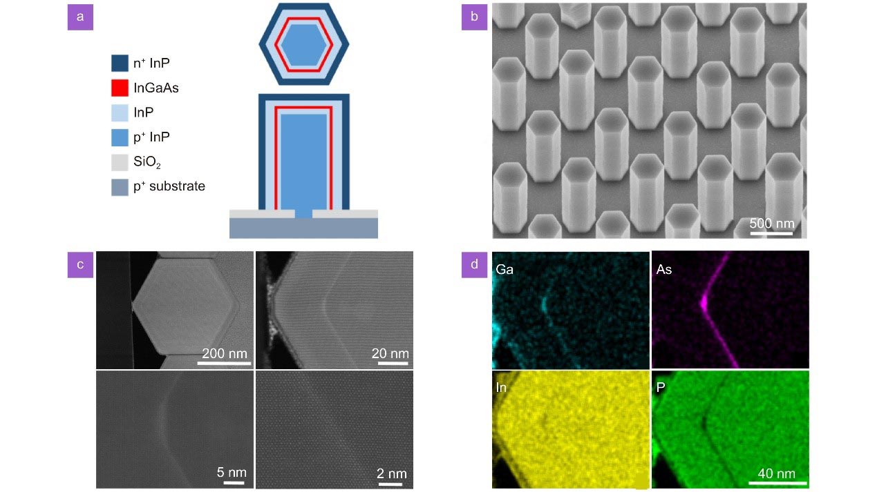
The authors of this article demonstrate the selective-area growth and fabrication of highly uniform p-i-n core-shell InGaAs/InP single quantum well (QW) nanowire array LEDs. Figure 1 (a, b) shows the schematic of the QW LED structure in a single nanowire and a scanning electron microscope (SEM) image of a nanowire array with highly uniform morphology, respectively. The detailed QW structure in the radial direction is further revealed by the high-angle annular dark-field scanning transmission electron microscopy (HAADF-STEM) image in Figure 1(c). To probe the material composition of the QW, the energy dispersive X-ray spectroscopy analysis in Figure 1(d) was also performed, clearly showing that the InGaAs QW region is gallium- and arsenic-rich compared to the InP barrier region.

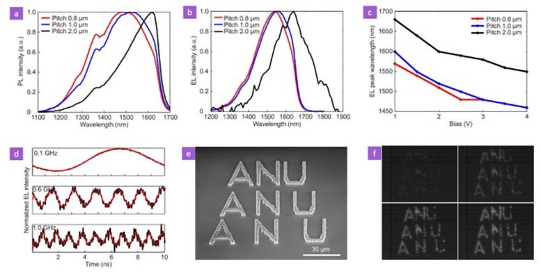
The QW nanowire LEDs exhibited strong bias-dependent electroluminescence (EL), shown in Figure 2 (c, d), covering telecommunication wavelengths (1.35~1.6 μm). Two prominent EL peaks can be identified from the spectra shown in Figure 2(d), including a long wavelength peak at ~1.5 μm originating from the radial QW and a short wavelength peak at ~1.35 μm due to a combined emission from axial and radial QWs. Due to the presence of two EL peaks, the full width at half-maximum of the EL spectrum could reach around 286 nm, showing great promise for optical coherence tomography and bio-sensing applications. With the increased bias, large carrier injection fills the energy bands in both QWs, leading to broadened emission spectra and a shift of the peak wavelength.
Tunability and Applications
The multi-wavelength tunability of the QW nanowire array has been further demonstrated through the monolithic growth of nanowire arrays with different pitch sizes (i.e., the center-to-center distance between neighboring nanowires in an array) on the same substrate.
Figure 3 (a) shows the representative photoluminescence (PL) spectra collected from nanowire arrays with different pitch sizes, showing longer wavelength PL emission from larger pitch nanowire arrays due to the increased QW thickness or indium incorporation into the QW.
The nanowire array LEDs with pitch sizes of 0.8, 1.0, and 2.0 μm were then fabricated on the same substrate, with the corresponding electroluminescence (EL) spectra at a bias of 1.5 V as shown in Figure 3 (b), showing a consistent trend as in the PL spectra. The EL emission from larger pitch nanowire array LED was observed at a longer wavelength, with the peak wavelength of the bias-dependent EL spectra extended from ~1.57 μm (pitch 0.8 μm array) to ~1.67 um (pitch 2.0 μm array), which covers the telecommunication C band.
Figure 3 (c) summarizes the bias-dependent (from 1 to 4 V) EL peak wavelength for all pitch sizes with more than 100 nm blueshift obtained for each case, indicating a broad emission wavelength tunability across the telecommunication wavelength regime.
The array-based QW nanowire LEDs also offer great potential for further boosting the communication capacity by integrating multiple multi-wavelength LEDs with much-reduced sizes on the same chip to achieve wavelength division multiplexing. As a proof of concept, multiple small-size micro-LED arrays with pixel sizes less than 5 µm arranged to the letters of “ANU” were grown under the same conditions used for large array growth shown in Figure 3(e). Several infrared camera images of multiple micro-LED arrays emitting under various biases are presented in Figure 3(f), highlighting the promise of integrating multiple multi-wavelength micro-LEDs on the same chip.
Conclusion
To conclude, the authors have demonstrated selective area growth and fabrication of highly uniform p-i-n core-shell InGaAs/InP single QW nanowire array micro-LEDs, with axial and radial QWs contributing to the electroluminescence at wavelengths of ~1.35 and 1.5 μm, respectively. The electroluminescence spectra of the nanowire array LED exhibited strong bias-dependent spectral shift due to the band-filling effect, indicating a voltage-controlled multi-wavelength (1.35–1.6 μm) operation covering telecommunication wavelengths.
The great compatibility of the nanowire array LEDs with wavelength-division-multiplexing and multiple-input multiple-output technologies for high-speed communication was further illustrated by the monolithic growth and fabrication of nanowire array LEDs with different pitch sizes and much-reduced array sizes (< 5 μm in width) on the same substrate, as well as GHz-level modulation. This work provides a promising pathway for developing nanoscale on-chip light sources for next-generation integrated optical communication systems.
Reference: “High-speed multiwavelength InGaAs/InP quantum well nanowire array micro-LEDs for next generation optical communications” by Fanlu Zhang, Zhicheng Su,
Zhe Li, Yi Zhu, Nikita Gagrani, Ziyuan Li, Mark Lockrey, Li Li, Igor Aharonovich, Yuerui Lu, Hark Hoe Tan, Chennupati Jagadish and Lan Fu, 26 June 2023, Opto-Electronic Science.
DOI: 10.29026/oes.2023.230003
Never miss a breakthrough: Join the SciTechDaily newsletter.
Follow us on Google and Google News.