Like restless children posing for a family portrait, electrons won’t hold still long enough to stay in any kind of fixed arrangement.
Now, a Cornell-led collaboration has developed a way to stack two-dimensional semiconductors and trap electrons in a repeating pattern that forms a specific and long-hypothesized crystal.
The team’s paper, “Correlated Insulating States at Fractional Fillings of Moiré Superlattices,” published on November 11, 2020, in Nature. The paper’s lead author is postdoctoral researcher Yang Xu.
The project grew out of the shared lab of Kin Fai Mak, associate professor of physics in the College of Arts and Sciences, and Jie Shan, professor of applied and engineering physics in the College of Engineering, the paper’s co-senior authors. Both researchers are members of the Kavli Institute at Cornell for Nanoscale Science; they came to Cornell through the provost’s Nanoscale Science and Microsystems Engineering (NEXT Nano) initiative.
A crystal of electrons was first predicted in 1934 by theoretical physicist Eugene Wigner. He proposed that when the repulsion that results from negatively charged electrons – called Coulomb repulsions – dominates the electrons’ kinetic energy, a crystal would form. Scientists have tried various methods to suppress that kinetic energy, such as putting electrons under an extremely large magnetic field, roughly a million times that of the Earth’s magnetic field. Complete crystallization remains elusive, but the Cornell team discovered a new method for achieving it.
“Electrons are quantum mechanical. Even if you don’t do anything to them, they’re spontaneously jiggling around all the time,” Mak said. “A crystal of electrons would actually have the tendency to just melt because it’s so hard to keep the electrons fixed at a periodic pattern.”
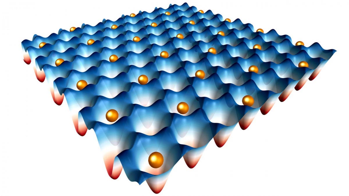
So the researchers’ solution was to build an actual trap by stacking two semiconductor monolayers, tungsten disulfide (WS2) and tungsten diselenide (WSe2), grown by partners at Columbia University. Each monolayer has a slightly different lattice constant. When paired together, they create a moiré superlattice structure, which essentially looks like a hexagonal grid. The researchers then placed electrons in specific sites in the pattern. As they found in an earlier project, the energy barrier between the sites locks the electrons in place.
“We can control the average occupancy of the electrons at a specific moiré site,” Mak said.
Given the intricate pattern of a moiré superlattice, combined with the jittery nature of electrons and the need to put them into a very specific arrangement, the researchers turned to Veit Elser, professor of physics and a co-author of the paper, who calculated the ratio of occupancy by which different arrangements of electrons will self-crystallize.
However, the challenge of Wigner crystals is not only creating them, but observing them, too.
“You need to hit just the right conditions to create an electron crystal, and at the same time, they’re also fragile,” Mak said. “You need a good way to probe them. You don’t really want to perturb them significantly while probing them.”
The team devised a new optical sensing technique in which an optical sensor is placed close to the sample, and the whole structure is sandwiched between insulating layers of hexagonal boron nitride, created by collaborators at the National Institute for Materials Science in Japan. Because the sensor is separated from the sample by about two nanometers, it doesn’t perturb the system.
The new technique enabled the team to observe numerous electron crystals with different crystal symmetries, from triangular-lattice Wigner crystals to crystals that self-aligned into stripes and dimers. By doing so, the team demonstrated how very simple ingredients can form complex patterns – as long as the ingredients sit still long enough.
Reference: “Correlated insulating states at fractional fillings of moiré superlattices” by Yang Xu, Song Liu, Daniel A. Rhodes, Kenji Watanabe, Takashi Taniguchi, James Hone, Veit Elser, Kin Fai Mak and Jie Shan, 11 November 2020, Nature.
DOI: 10.1038/s41586-020-2868-6
The paper’s co-authors include researchers from Columbia University and the National Institute for Materials Science in Japan.
The research and device fabrication were supported by the U.S. Department of Energy, the U.S. Office of Naval Research and the David and Lucille Packard Fellowship.
Never miss a breakthrough: Join the SciTechDaily newsletter.
Follow us on Google and Google News.