A team from EPFL and NCCR Marvel has identified more than 1,000 materials with a particularly interesting 2D structure. Their research, which made the cover page of Nature Nanotechnology, paves the way for groundbreaking technological applications.
2D materials, which consist of a few layers of atoms, may well be the future of nanotechnology. They offer potential new applications and could be used in small, higher-performance, and more energy-efficient devices. 2D materials were first discovered almost 15 years ago, but only a few dozen of them have been synthesized so far. Now, thanks to an approach developed by researchers from EPFL’s Theory and Simulation of Materials Laboratory (THEOS) and from NCCR-MARVEL for Computational Design and Discovey of Novel Materials, many more promising 2D materials may now be identified. Their work was recently published in the journal Nature Nanotechnology, and even got a mention on the cover page.
The first 2D material to be isolated was graphene, in 2004, earning the researchers who discovered it a Nobel Prize in 2010. This marked the start of a whole new era in electronics, as graphene is light, transparent and resilient, and, above all, a good conductor of electricity. It paved the way to new applications in numerous fields such as photovoltaics and optoelectronics.
“To find other materials with similar properties, we focused on the feasibility of exfoliation,” explains Nicolas Mounet, a researcher in the THEOS lab and lead author of the study. “But instead of placing adhesive strips on graphite to see if the layers peeled off, like the Nobel Prize winners did, we used a digital method.”
More than 100,000 materials analyzed
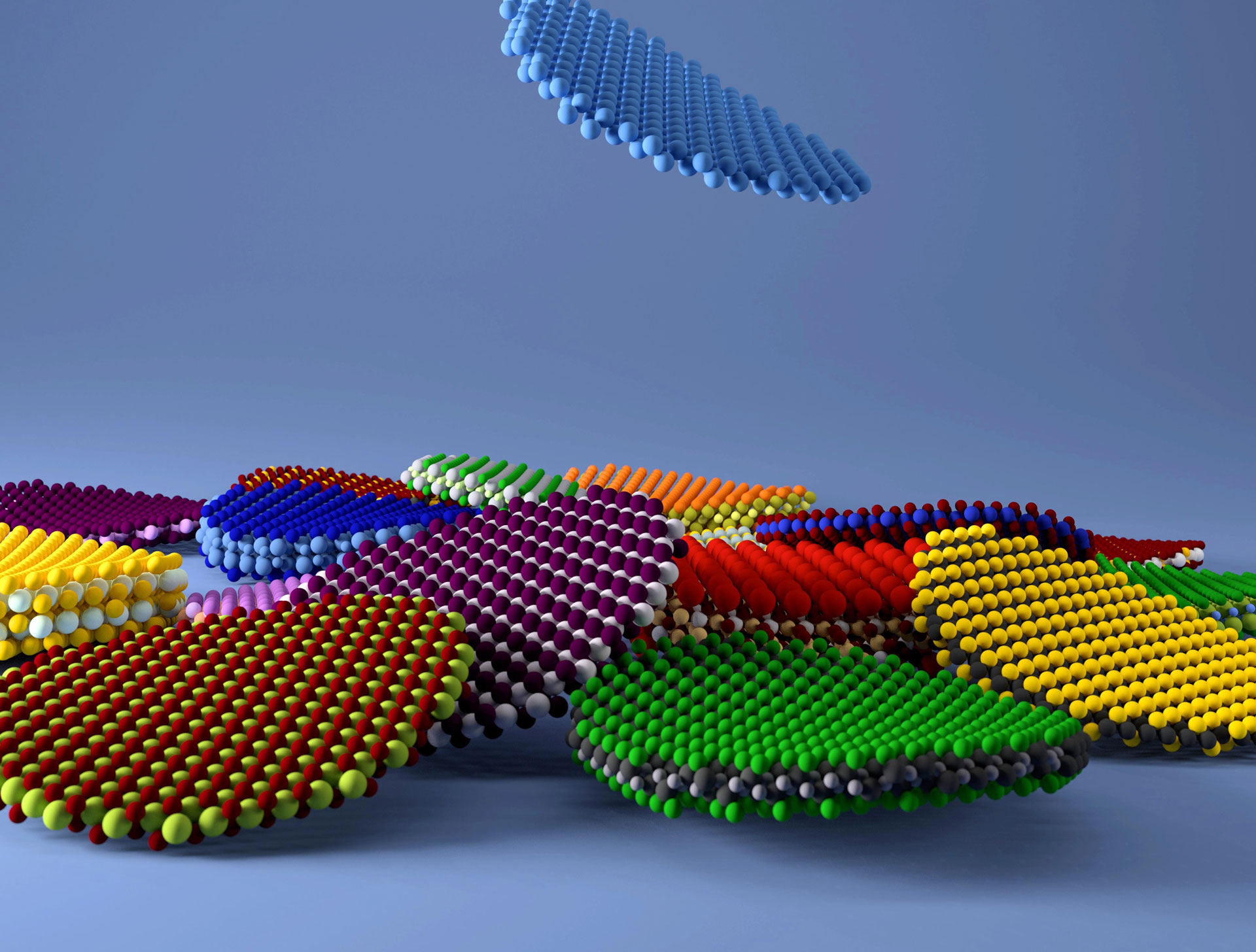
The researchers developed an algorithm to review and carefully analyze the structure of more than 100,000 3D materials recorded in external databases. From this, they created a database of around 5,600 potential 2D materials, including more than 1,000 with particularly promising properties. In other words, they’ve created a treasure trove for nanotechnology experts.
To build their database, the researchers used a step-by-step process of elimination. First, they identified all of the materials that are made up of separate layers. “We then studied the chemistry of these materials in greater detail and calculated the energy that would be needed to separate the layers, focusing primarily on materials where interactions between atoms of different layers are weak, something known as Van der Waals bonding,” says Marco Gibertini, a researcher at THEOS and the second author of the study.
A plethora of 2D candidates
Of the 5,600 materials initially identified, the researchers singled out 1,800 structures that could potentially be exfoliated, including 1,036 that looked especially easy to exfoliate. This represents a considerable increase in the number of possible 2D materials known today. They then selected the 258 most promising materials, categorizing them according to their magnetic, electronic, mechanical, thermal, and topological properties.
“Our study demonstrates that digital techniques can really boost discoveries of new materials,” says Nicola Marzari, the director of NCCR Marvel and a professor at THEOS. “In the past, chemists had to start from scratch and just keep trying different things, which required hours of lab work and a certain amount of luck. With our approach, we can avoid this long, frustrating process because we have a tool that can single out the materials that are worth studying further, allowing us to conduct more focused research.”
It is also possible to reproduce the researchers’ calculations thanks to their software AiiDA, which describes the calculation process for each material discovered in the form of workflows and stores the full provenance of each stage of the calculation. “Without AiiDA, it would have been very difficult to combine and process different types of data,” explains Giovanni Pizzi, a senior researcher at THEOS and co-author of the study. “Our workflows are available to the public, so anyone in the world can reproduce our calculations and apply them to any material to find out if it can be exfoliated.”
Reference: “Two-dimensional materials from high-throughput computational exfoliation of experimentally known compounds” by Nicolas Mounet, Marco Gibertini, Philippe Schwaller, Davide Campi, Andrius Merkys, Antimo Marrazzo, Thibault Sohier, Ivano Eligio Castelli, Andrea Cepellotti, Giovanni Pizzi and Nicola Marzari, 6 February 2018, Nature Nanotechnology.
DOI: 10.1038/s41565-017-0035-5
Never miss a breakthrough: Join the SciTechDaily newsletter.
Follow us on Google and Google News.