SMART findings allow a new way to control light emitting from materials.
Researchers from the Low Energy Electronic Systems (LEES) interdisciplinary research group at the Singapore-MIT Alliance for Research and Technology (SMART), MIT’s research enterprise in Singapore, together with MIT and National University of Singapore (NUS), have discovered a new way to control light emission from materials.
Controlling the properties of materials has been the driving force behind many modern technologies — from solar panels to computers, smart vehicles, and lifesaving hospital equipment. But materials properties have traditionally been adjusted based on their composition, structure, and sometimes size, and most practical devices that produce or generate light use layers of materials of different compositions that can often be difficult to grow.
A New Approach Using Twist Angles
The breakthrough by SMART researchers and their collaborators offers a new paradigm-shifting approach to tune the optical properties of technologically relevant materials by changing the twist angle between stacked films, at room temperature. Their findings could have a huge impact on various applications in the medical, biological, and quantum information fields. The team explain their research in a paper titled “Tunable Optical Properties of Thin Films Controlled by the Interface Twist Angle,” published recently in Nano Letters.
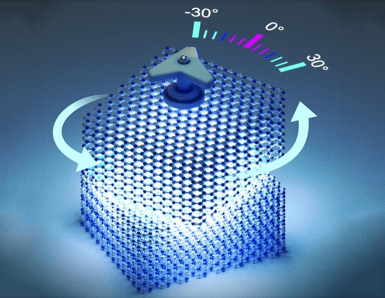
“A number of new physical phenomena — such as unconventional superconductivity — have been discovered recently by stacking individual layers of atomically-thin materials on top of each other at a twist angle, which results in the formation of what we call moiré superlattices,” says corresponding author of the paper Professor Silvija Gradecak from the Department of Materials Science and Engineering at NUS and principal investigator at SMART LEES. “The existing methods focus on stacking only thin individual monolayers of film, which is laborious, while our discovery would be applicable to thick films as well — making the process of materials discovery much more efficient.”
Their research can also be meaningful for developing the fundamental physics in the field of “twistronics” — the study of how the angle between layers of two-dimensional materials can change their electrical properties. Gradecak points out that the field has so far focused on stacking individual monolayers, which requires careful exfoliation and may suffer from relaxation from a twisted state, thus limiting their practical applications. The team’s discovery could make this groundbreaking twist-related phenomenon applicable to thick film systems as well, which are easy to manipulate and industrially relevant.
Room-Temperature Moiré Tuning in Thick Films
“Our experiments showed that the same phenomena leading to the formation of moiré superlattices in two-dimensional systems can be translated to tune optical properties of three-dimensional, bulk-like hexagonal boron nitride (hBN), even at room temperature,” says Hae Yeon Lee, the lead author of the paper and a materials science and engineering PhD candidate at MIT. “We found that both the intensity and color of stacked, thick hBN films can be continuously tuned by their relative twist angles and intensity increased by more than 40 times.”
The research results open up a new way to control optical properties of thin films beyond the conventionally used structures, especially for applications in medicine and environmental or information technologies.
Reference: “Tunable Optical Properties of Thin Films Controlled by the Interface Twist Angle” by Hae Yeon Lee, Mohammed M. Al Ezzi, Nimisha Raghuvanshi, Jing Yang Chung, Kenji Watanabe, Takashi Taniguchi, Slaven Garaj, Shaffique Adam and Silvija Gradečak, 16 February 2021, Nano Letters.
DOI: 10.1021/acs.nanolett.0c04924
The research is carried out by SMART and supported by the National Research Foundation (NRF) Singapore under its Campus for Research Excellence And Technological Enterprise (CREATE) program.
LEES is creating new integrated circuit technologies that result in increased functionality, lower power consumption, and higher performance for electronic systems. These integrated circuits of the future will impact applications in wireless communications and power electronics, LED lighting, and displays. LEES has a vertically-integrated research team possessing expertise in materials, devices, and circuits, comprising multiple individuals with professional experience within the semiconductor industry. This ensures that the research is targeted to meet the needs of the semiconductor industry both within Singapore and globally.
SMART was established by MIT in partnership with the NRF in 2007. SMART is the first entity in CREATE. SMART serves as an intellectual and innovation hub for cutting-edge research projects in areas of interest to both Singapore and MIT. It currently comprises an Innovation Center and five interdisciplinary research group: Antimicrobial Resistance, Critical Analytics for Manufacturing Personalized-Medicine, Disruptive and Sustainable Technologies for Agricultural Precision, Future Urban Mobility, and LEES.
SMART research is funded by the NRF under the CREATE program.
Never miss a breakthrough: Join the SciTechDaily newsletter.
Follow us on Google and Google News.