
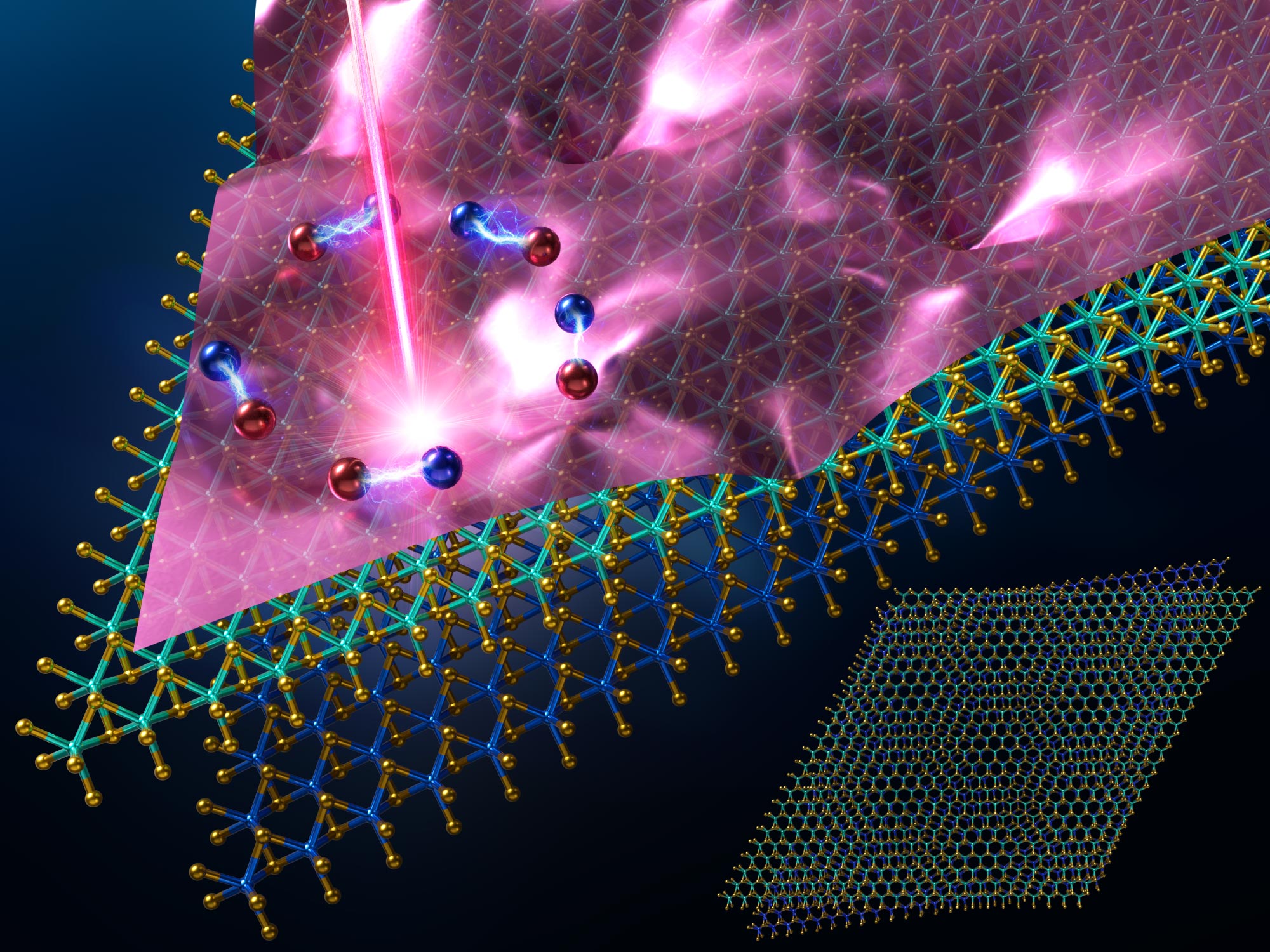
A study of twisted two-dimensional semiconductors reveals how subtle material disorder can emerge at different spatial scales.
Two distinct forms of hidden disorder may influence how ultrathin semiconductors emit light. One extends across relatively large areas of the material, while the other is concentrated around tiny defects. A new theoretical approach offers a way to identify these patterns by analyzing changes in light emission rather than attempting to separate individual spectral signals.
Developed by Katsunori Wakabayashi at the Research Center for Materials Nanoarchitectonics (MANA), part of the National Institute for Materials Science (NIMS), the framework could provide a more reliable way to investigate imperfections in materials used for advanced optical and quantum devices.
Why Twisted Semiconductor Layers Are Difficult to Analyze
The research examines moiré heterostructures, which form when two extremely thin semiconductor layers are stacked with a slight rotational misalignment. In materials such as molybdenum diselenide and tungsten diselenide (MoSe2/WSe2), this arrangement creates a repeating moiré pattern that alters how the combined layers interact with and emit light.
These structures produce complex photoluminescence spectra containing numerous overlapping emission peaks. Scientists typically study such spectra by identifying individual peaks and determining their physical origins. However, the dense, overlapping signals in moiré heterostructures make those assignments difficult and potentially uncertain.
Using Light to Map Hidden Material Disorder
Wakabayashi developed a mathematical framework that examines how simpler spectral properties, including peak energy and average emission energy, change across a material’s surface. Applying the approach to previously reported spectral correlations in a MoSe2/WSe2 heterostructure suggested that different optical features respond to different scales of structural disorder.
The analysis identified two possible components of this hidden disorder. The first is a smoothly varying ‘background’ extending over distances of a few micrometers (roughly 0.0001 inch). The second is much more localized and may arise from small defects or sites where excitons become trapped. Excitons are bound pairs of electrons and positively charged holes that can release energy as light.
By comparing spatial variations in the spectral measurements with theoretical predictions, the framework makes it possible to infer the underlying disorder without assigning an origin to every emission peak. This approach could eventually help researchers evaluate material quality and improve the consistency of semiconductor manufacturing.
“This work could help researchers make better and more reproducible materials for light-emitting devices, optical sensors, and quantum technologies,” remarks Wakabayashi.
Reference: “Hierarchical disorder in moiré exciton photoluminescence probed by spectral-descriptor correlations” by Katsunori Wakabayashi, 7 August 2026, Physical Review Research.
DOI: 10.1103/jt25-c8fp
Never miss a breakthrough: Join the SciTechDaily newsletter.
Follow us on Google and Google News.