
Researchers at Rice University have shown the ability to pattern a conductor (graphene) and insulator (hexagonal boron nitride) into a one-atom-thick hybrid of graphene and hexagonal boron nitride, an important step toward the creation of two-dimensional electronics.
Rice University scientists have taken an important step toward the creation of two-dimensional electronics with a process to make patterns in atom-thick layers that combine a conductor and an insulator.
The materials at play – graphene and hexagonal boron nitride – have been merged into sheets and built into a variety of patterns at nanoscale dimensions.
Rice introduced a technique to stitch the identically structured materials together nearly three years ago. Since then, the idea has received a lot of attention from researchers interested in the prospect of building 2D, atomic-layer circuits, said Rice materials scientist Pulickel Ajayan. He is one of the authors of the new work that appears this week in Nature Nanotechnology. In particular, Ajayan noted that Cornell University scientists reported an advance late last year on the art of making atomic-layer heterostructures through sequential growth schemes.
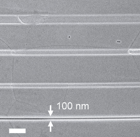
This week’s contribution by Rice offers manufacturers the possibility of shrinking electronic devices into even smaller packages. While Rice’s technical capabilities limited features to a resolution of about 100 nanometers, the only real limits are those defined by modern lithographic techniques, according to the researchers. (A nanometer is one-billionth of a meter.)
“It should be possible to make fully functional devices with circuits 30, even 20 nanometers wide, all in two dimensions,” said Rice researcher Jun Lou, a co-author of the new paper. That would make circuits on about the same scale as in current semiconductor fabrication, he said.
Graphene has been touted as a wonder material since its discovery in the last decade. Even at one atom thick, the hexagonal array of carbon atoms has proven its potential as a fascinating electronic material. But to build a working device, conductors alone will not do. Graphene-based electronics require similar, compatible 2D materials for other components, and researchers have found hexagonal boron nitride (h-BN) works nicely as an insulator.
H-BN looks like graphene, with the same chicken-wire atomic array. The earlier work at Rice showed that merging graphene and h-BN via chemical vapor deposition (CVD) created sheets with pools of the two that afforded some control of the material’s electronic properties. Ajayan said at the time that the creation offered “a great playground for materials scientists.”
He has since concluded that the area of two-dimensional materials beyond graphene “has grown significantly and will play out as one of the key exciting materials in the near future.”
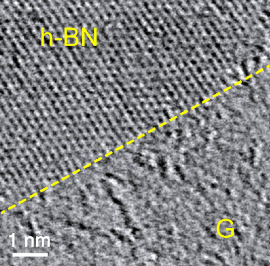
His prediction bears fruit in the new work, in which finely detailed patterns of graphene are laced into gaps created in sheets of h-BN. Combs, bars, concentric rings and even microscopic Rice Owls were laid down through a lithographic process. The interface between elements, seen clearly in scanning transmission electron microscope images taken at the Oak Ridge National Laboratory, shows a razor-sharp transition from graphene to h-BN along a subnanometer line.
“This is not a simple quilt,” Lou said. “It’s very precisely engineered. We can control the domain sizes and the domain shapes, both of which are necessary to make electronic devices.”
The new technique also began with CVD. Lead author Zheng Liu, a Rice research scientist, and his colleagues first laid down a sheet of h-BN. Laser-cut photoresistant masks were placed over the h-BN, and exposed material was etched away with argon gas. (A focused ion beam system was later used to create even finer patterns, down to 100-nanometer resolution, without masks.) After the masks were washed away, graphene was grown via CVD in the open spaces, where it bonded edge-to-edge with the h-BN. The hybrid layer could then be picked up and placed on any substrate.
While there’s much work ahead to characterize the atomic bonds where graphene and h-BN domains meet and to analyze potential defects along the boundaries, Liu’s electrical measurements proved the components’ qualities remain intact.
“One important thing Zheng showed is that even by doing all kinds of growth, then etching, then regrowth, the intrinsic properties of these two materials are not affected,” Lou said. “Insulators stay insulators; they’re not doped by the carbon. And the graphene still looks very good. That’s important, because we want to be sure what we’re growing is exactly what we want.”
Liu said the next step is to place a third element, a semiconductor, into the 2D fabric. “We’re trying very hard to integrate this into the platform,” he said. “If we can do that, we can build truly integrated in-plane devices.” That would give new options to manufacturers toying with the idea of flexible electronics, he said.
“The contribution of this paper is to demonstrate the general process,” Lou added. “It’s robust, it’s repeatable and it creates materials with very nice properties and with dimensions that are at the limit of what is possible.”
Reference: “In-plane heterostructures of graphene and hexagonal boron nitride with controlled domain sizes” by Zheng Liu, Lulu Ma, Gang Shi, Wu Zhou, Yongji Gong, Sidong Lei, Xuebei Yang, Jiangnan Zhang, Jingjiang Yu, Ken P. Hackenberg, Aydin Babakhani, Juan-Carlos Idrobo, Robert Vajtai, Jun Lou and Pulickel M. Ajayan, 27 January 2013, Nature Nanotechnology.
DOI: 10.1038/nnano.2012.256
Co-authors of the paper are graduate students Lulu Ma, Gang Shi, Yongji Gong, Ken Hackenberg, Sidong Lei and Jiangnan Zhang; Aydin Babakhani, an assistant professor of electrical and computer engineering; and Robert Vajtai, a faculty fellow in mechanical engineering and materials science, all at Rice; Wu Zhou, a research associate at Vanderbilt University and Wigner Fellow at Oak Ridge National Laboratory; Xuebei Yang, a former research assistant at Rice, now at Agilent Technologies; Jingjiang Yu, a scientist at Agilent Technologies; and Juan-Carlos Idrobo, a research professor of physics at Vanderbilt and a guest scientist at Oak Ridge. Lou is an associate professor of mechanical engineering and materials science. Ajayan is the Benjamin M. and Mary Greenwood Anderson Professor in Mechanical Engineering and Materials Science and of chemistry at Rice.
The work was supported by U.S. Army Research Office and U.S. Office of Naval Research Multidisciplinary University Research Initiative grants; the Nanoelectronics Research Corp; a U.S.-Japan Cooperative Research and Education in Terahertz grant; the Welch Foundation; the National Science Foundation; and Oak Ridge National Laboratory’s Shared Research Equipment User Program, sponsored by the Office of Basic Energy Sciences, U.S. Department of Energy.
Never miss a breakthrough: Join the SciTechDaily newsletter.
Follow us on Google and Google News.
1 Comment
They said one atom think so how is that 2d in anyway shape or form