Close Menu
    Facebook X (Twitter) Instagram
    SciTechDaily
    • Biology
    • Chemistry
    • Earth
    • Health
    • Physics
    • Science
    • Space
    • Technology
    Facebook X (Twitter) Pinterest YouTube RSS
    SciTechDaily
    Home»Technology»EPFL Creates Memory Cell by Combining Molybdenite and Graphene
    Technology

    EPFL Creates Memory Cell by Combining Molybdenite and Graphene

    By Ecole Polytechnique Federale de Lausanne, EPFLMarch 21, 2013No Comments4 Mins Read
    Facebook Twitter Pinterest Telegram LinkedIn WhatsApp Email Reddit
    Share
    Facebook Twitter LinkedIn Pinterest Telegram Email Reddit
    Memory Cell by Combining Molybdenite and Graphene
    EPFL scientists have combined two materials with advantageous electronic properties – graphene and molybdenite – into a flash memory prototype that is very promising in terms of performance, size, flexibility and energy consumption. Credit: EPFL

    EPFL scientists have combined monolayer MoS2 with graphene to build a flash memory prototype capable of information storage.

    EPFL scientists have combined two materials with advantageous electronic properties – graphene and molybdenite – into a flash memory prototype that is promising in terms of performance, size, flexibility, and energy consumption.

    After the molybdenite chip, we now have molybdenite flash memory, a significant step forward in the use of this new material in electronics applications. The news is even more impressive because scientists from EPFL’s Laboratory of Nanometer Electronics and Structures (LANES) came up with a truly original idea: they combined the advantages of this semiconducting material with those of another amazing material – graphene.

    The results of their research have recently been published in the journal ACS Nano.

    Molybdenite and Graphene Memory Cell
    MoS2/graphene heterostructure memory layout. (a) Three-dimensional schematic view of the memory device based on single-layer MoS2. (b) Schematics of a heterostructure memory cell with a single-layer MoS2 semiconducting channel, graphene contacts and multilayer graphene (MLG) floating gate. The MLG floating gate is separated from the channel by a thin tunneling oxide (ca. 1 nm Al2O3 + 6 nm HfO2) and from the control gate by a thicker blocking oxide (1 nm Al2O3 + 30 nm HfO2). (c) Optical micrographs of two graphene/MoS2 heterostructure transistors fabricated on the same MoS2 monolayer flake at various stages of fabrication. Left: single-layer MoS2 transferred over an array of graphene stripes patterned on oxidized silicon chips and contacted with metal leads (Cr/Au: 10/50 nm); middle: the same device after deposition of the tunneling oxide and transfer/patterning of MLG floating gates; right: final device after the deposition of the blocking oxide and definition of the control gate electrodes (Cr/Au: 10/50 nm). Scale bars: 3 μm. Credit: Simone Bertolazzi et al., ACS Nano, DOI: 10.1021/nn3059136

    Two years ago, the LANES team revealed the promising electronic properties of molybdenite (MoS2), a mineral that is very abundant in nature. Several months later, they demonstrated the possibility of building an efficient molybdenite chip. Today, they’ve gone further still by using it to develop a flash memory prototype – that is, a cell that can not only store data but also maintain it in the absence of electricity. This is the kind of memory used in digital devices such as cameras, phones, laptop computers, printers, and USB keys.

    An ideal “energy band”

    “For our memory model, we combined the unique electronic properties of MoS2 with graphene’s amazing conductivity,” explains Andras Kis, author of the study and director of LANES.

    Molybdenite and graphene have many things in common. Both are expected to surpass the physical limitations of our current silicon chips and electronic transistors. Their two-dimensional chemical structure – the fact that they’re made up of a layer only a single atom thick – gives them huge potential for miniaturization and mechanical flexibility.

    Although graphene is a better conductor, molybdenite has advantageous semi-conducting properties. MoS2 has an ideal “energy band” in its electronic structure that graphene does not. This allows it to switch very easily from an “on” to an “off” state, and thus to use less electricity. Used together, the two materials can thus combine their unique advantages.

    Like a sandwich

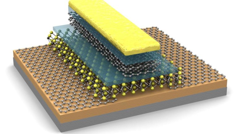
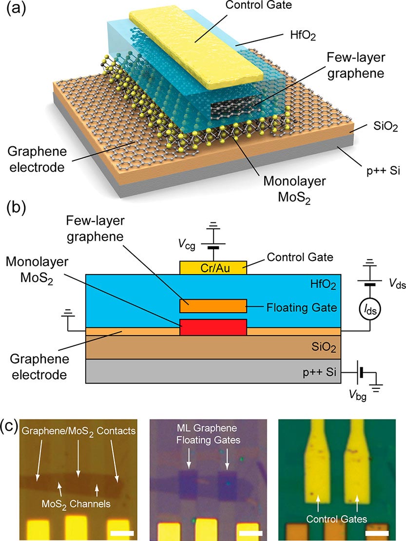
    The transistor prototype developed by LANES was designed using “field effect” geometry, a bit like a sandwich. In the middle, instead of silicon, a thin layer of MoS2 channels electrons. Underneath, the electrodes transmitting electricity to the MoS2 layer are made out of graphene. And on top, the scientists also included an element made up of several layers of graphene; this captures electric charge and thus stores memory.

    “Combining these two materials enabled us to make great progress in miniaturization, and also using these transistors we can make flexible nanoelectronic devices,” explains Kis. The prototype stores a bit of memory, just like a traditional cell. But according to the scientist, because molybdenite is thinner than silicon and thus more sensitive to charge, it offers great potential for more efficient data storage.

    Reference: “Nonvolatile Memory Cells Based on MoS2/Graphene Heterostructures” by Simone Bertolazzi, Daria Krasnozhon and Andras Kis, 19 March 2013, ACS Nano.
    DOI: 10.1021/nn3059136

    Never miss a breakthrough: Join the SciTechDaily newsletter.
    Follow us on Google and Google News.

    EPFL Graphene Materials Science Memory Chips Nanotechnology
    Share. Facebook Twitter Pinterest LinkedIn Email Reddit

    Related Articles

    Patterning Graphene With Metallized DNA Nanolithography

    A Cost-Effective Fabrication Method for Micro-Scale Graphene-Based Supercapacitors

    Triangular Layers of Tungsten Disulfide May Have Applications in Optical Technology

    Growing Graphene Without the Defects

    A Step Towards 2D Devices, Hybrid Graphene/Hexagonal Boron Nitride

    Controlled Graphene Crumpling Used as Artificial Muscle Actuators

    New 3D Form of Graphene May Lead to Flexible Electronics

    “Patterned Regrowth” May Lead to Graphene-Based Circuits

    3D Self-Assembling Polymer Materials Could Lead to New Microchips

    Leave A Reply Cancel Reply

    • Facebook
    • Twitter
    • Pinterest
    • YouTube

    Don't Miss a Discovery

    Subscribe for the Latest in Science & Tech!

    Trending News

    Your Blood Pressure Reading Could Be Wrong Because of One Simple Mistake

    Astronomers Stunned by Ancient Galaxy With No Spin

    Physicists May Be on the Verge of Discovering “New Physics” at CERN

    Scientists Solve 320-Million-Year Mystery of Reptile Skin Armor

    Scientists Say This Daily Walking Habit May Be the Secret to Keeping Weight Off After Dieting

    New Therapy Rewires the Brain To Restore Joy in Depression Patients

    Giant Squid Detected off Western Australia in Stunning Deep-Sea Discovery

    Popular Sugar-Free Sweetener Linked to Liver Disease, Study Warns

    Follow SciTechDaily
    • Facebook
    • Twitter
    • YouTube
    • Pinterest
    • Newsletter
    • RSS
    SciTech News
    • Biology News
    • Chemistry News
    • Earth News
    • Health News
    • Physics News
    • Science News
    • Space News
    • Technology News
    Recent Posts
    • Scientists Say Cognitive Decline Isn’t Inevitable — Your Brain Can Improve at Any Age
    • This Weird Sea Creature May Have Rewritten Life’s Genetic Rulebook
    • The Hidden Types of Dementia Most People Have Never Heard Of
    • Scientists Discover Why Alcohol Prevents the Liver From Healing, Even After You Quit
    • Scientists Solve a 60-Year-Old Fat Cell Mystery — and It Changes What We Know About Obesity
    Copyright © 1998 - 2026 SciTechDaily. All Rights Reserved.
    • Science News
    • About
    • Contact
    • Editorial Board
    • Privacy Policy
    • Terms of Use

    Type above and press Enter to search. Press Esc to cancel.