
Researchers devise an approach to vastly enhance the near-infrared absorption in silicon, which could lead to affordable, high-performance photonic devices.
Photonic systems are swiftly gaining momentum in numerous emerging applications, including optical communications, lidar sensing, and medical imaging. However, the general acceptance of photonics in future engineering solutions depends heavily on the cost of manufacturing photodetectors, which is largely determined by the type of semiconductor used.
Traditionally, silicon (Si) has been the dominant semiconductor in the electronics industry. As a result, the majority of the industry has evolved around this material. However, Si has a relatively low light absorption coefficient in the near-infrared (NIR) spectrum compared to other semiconductors such as gallium arsenide (GaAs). Due to this, GaAs and similar alloys are more effective in photonic applications, but they don’t align with traditional complementary metal-oxide-semiconductor (CMOS) processes used in the majority of electronics production. This incompatibility leads to a significant increase in their manufacturing costs.
Novel Approach to Photodetector Design
In response to this issue, a research team from UC Davis in California is developing a novel strategy to dramatically enhance the light absorption of thin Si films. Their latest paper, published in the jouranl Advanced Photonics Nexus, presents the first experimental demonstration of Si-based photodetectors with light-trapping micro- and nano-surface structures. This approach has achieved performance improvements that match those of GaAs and other group III-V semiconductors.
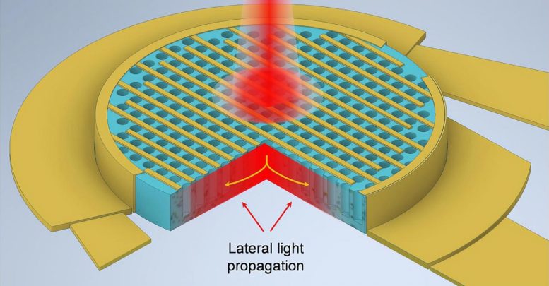
The proposed photodetectors consist of a micrometer-thick cylindrical Si slab placed over an insulating substrate, with metallic “fingers” extending from the contact metals atop the slab in an interdigitated fashion. Importantly, the bulk Si is filled with circular holes arranged in a periodic pattern that act as photon-trapping sites. The overall structure of the device causes normally incident light to bend by almost 90° upon hitting the surface, making it travel laterally along the Si plane. These laterally propagating modes increase the propagation length of light and effectively slow it down, leading to more light–matter interaction and a consequent increase in absorption.
Analysis and Findings
The researchers additionally conducted optical simulations and theoretical analyses to better understand the effects of the photon-trapping structures, and performed several experiments comparing photodetectors with and without them. They found that photon trapping led to a remarkable increase in the absorption efficiency over a wide band in the NIR spectrum, staying above 68 percent and peaking at 86 percent.
Notably, the observed absorption coefficient of the photon-trapping photodetector was several times higher than that of plain Si and exceeded that of GaAs in the NIR band. Furthermore, although the proposed design was for a 1-μm-thick Si slab, simulations of 30- and 100-nm Si thin films compatible with CMOS electronics showed a similarly enhanced performance.
Conclusion and Future Implications
Overall, this study’s findings illustrate a promising strategy to enhance the performance of Si-based photodetectors for upcoming photonics applications. By attaining high absorption even in ultra-thin Si layers, the parasitic capacitance of the circuit can remain low, a critical factor in high-speed systems. Additionally, the proposed method aligns with modern CMOS manufacturing processes, potentially revolutionizing the way optoelectronics are integrated into conventional circuits. This could eventually lead to affordable ultra-fast computer networks and substantial advancements in imaging technology.
Reference: “Achieving higher photoabsorption than group III-V semiconductors in ultrafast thin silicon photodetectors with integrated photon-trapping surface structures” by Wayesh Qarony, Ahmed S. Mayet, Ekaterina Ponizovskaya-Devine, Soroush Ghandiparsi, Cesar Bartolo-Perez, Ahasan Ahamed, Amita Rawat, Hasina H. Mamtaz, Toshishige Yamada, Shih-Yuan Wang and M. Saif Islam, 24 July 2023, Advanced Photonics Nexus.
DOI: 10.1117/1.APN.2.5.056001
Never miss a breakthrough: Join the SciTechDaily newsletter.
Follow us on Google and Google News.