A newly published study details how graphene can be used in photodetectors to convert optical signals to electrical signals in integrated optoelectronic computer chips.
Graphene — which consists of atom-thick sheets of carbon atoms arranged hexagonally — is the new wonder material: Flexible, lightweight, and incredibly conductive electrically, it’s also the strongest material known to man.
In the latest issue of Nature Photonics, researchers at MIT, Columbia University, and IBM’s T. J. Watson Research Center describe a promising new application of graphene, photodetectors that would convert optical signals to electrical signals in integrated optoelectronic computer chips. Using light rather than electricity to move data both within and between computer chips could drastically reduce their power consumption and heat production, problems that loom ever larger as chips’ computational capacity increases.
Optoelectronic devices built from graphene could be much simpler in design than those made from other materials. If a method for efficiently depositing layers of graphene — a major area of research in materials science — can be found, it could ultimately lead to optoelectronic chips that are simpler and cheaper to manufacture.
“Another advantage, besides the possibility of making device fabrication simpler, is that the high mobility and ultrahigh carrier-saturation velocity of electrons in graphene makes for very fast detectors and modulators,” says Dirk Englund, the Jamieson Career Development Assistant Professor of Electrical Engineering and Computer Science at MIT, who led the new research.
Graphene is also responsive to a wider range of light frequencies than the materials typically used in photodetectors, so graphene-based optoelectronic chips could conceivably use a broader-band optical signal, enabling them to move data more efficiently. “A two-micron photon just flies straight through a germanium photodetector,” Englund says, “but it is absorbed and leads to measurable current — as we actually show in the paper — in graphene.”
Unbiased account
As Englund explains, the problem with graphene as a photodetector has traditionally been its low responsivity: A sheet of graphene will convert only about 2 percent of the light passing through it into an electrical current. That’s actually quite high for a material only an atom thick, but it’s still too low to be useful.
When light strikes a photoelectric material like germanium or graphene, it kicks electrons orbiting atoms of the material into a higher energy state, where they’re free to flow in an electrical current. If they don’t immediately begin to move, however, they’ll usually drop back down into the lower energy state. So one standard trick for increasing a photodetector’s responsivity is to “bias” it — to apply a voltage across it that causes the electrons to flow before they lose energy.
The problem is that the voltage will inevitably induce a slight background current that adds “noise” to the detector’s readings, making them less reliable. So Englund, his student Ren-Jye Shiue, Columbia’s Xuetao Gan — who, together with Shiue, is the lead author on the paper — and their collaborators instead used a photodetector design developed by Fengnian Xia and his colleagues at IBM, which produces a slight bias without the application of a voltage.
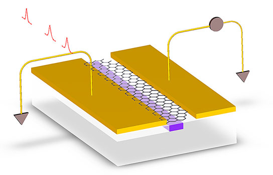
In the new design, light enters the detector through a silicon channel — a “waveguide” — etched into the surface of a chip. The layer of graphene is deposited on top of and perpendicular to the waveguide. On either side of the graphene layer is a gold electrode. But the electrodes’ placement is asymmetrical: One of them is closer to the waveguide than the other.
“There’s a mismatch between the energy of electrons in the metal contact and in graphene,” Englund says, “and this creates an electric field near the electrode.” When electrons are kicked up by photons in the waveguide, the electric field pulls them to the electrode, creating a current.
Hot topic
In experiments, the researchers found that, unbiased, their detector would generate 16 milliamps of current for each watt of incoming light. Its detection frequency was 20 gigahertz — already competitive with germanium. (Some experimental germanium photodetectors have achieved higher speeds, but only when biased.) With the application of a slight bias, the detector could get up to 100 milliamps per watt, a responsivity commensurate with that of germanium.
Englund is confident that better engineering — thinner electrodes, or a narrower waveguide — could yield a photodetector whose responsivity is even higher. “It’s a matter of engineering,” he says. “We are already testing some new tricks to get another factor of two or four.”
“I think it’s great work,” says Thomas Mueller, an assistant professor at the Vienna University of Technology’s Photonics Institute. “The main drawback of graphene photodetectors was always their low responsivity. Now they have two orders of magnitude higher responsivity, which is really great.”
“The other thing that I like very much is the integration with a silicon chip,” Mueller adds, “which really shows that, in the end, you’ll be able to integrate graphene into computer chips to realize optical links and things like that.”
In fact, the same issue of Nature Photonics also features a paper by Mueller and colleagues, reporting work very similar to that conducted by Englund and his team. “We did not know that we were doing the same thing,” Mueller says. “But I’m very happy that two papers are coming out in the same journal on the same topic, which shows that it’s an important thing, I think.”
The chief difference between the two groups’ work, Mueller says, is that “we used slightly different geometry.” But, he adds, “Honestly, I think that Dirk’s geometry is more practical. We were also thinking about the same thing, but we didn’t have the technical capabilities to do this. There’s one process that they do that we were not able to do.”
Reference: “Chip-integrated ultrafast graphene photodetector with high responsivity” by Xuetao Gan, Ren-Jye Shiue, Yuanda Gao, Inanc Meric, Tony F. Heinz, Kenneth Shepard, James Hone, Solomon Assefa and Dirk Englund, 15 September 2013, Nature Photonics.
DOI: 10.1038/nphoton.2013.253
Never miss a breakthrough: Join the SciTechDaily newsletter.
Follow us on Google and Google News.
1 Comment
I’ve often wondered why solar panels can´t be biased with a couple of KV instead of just being sprinkled with a bit of boron… in a power production application wouldn´t any “backround noise” current from the overstrained crystal be a useful addition to any current generated by incident photons? sorry but it just seems too obvious…