
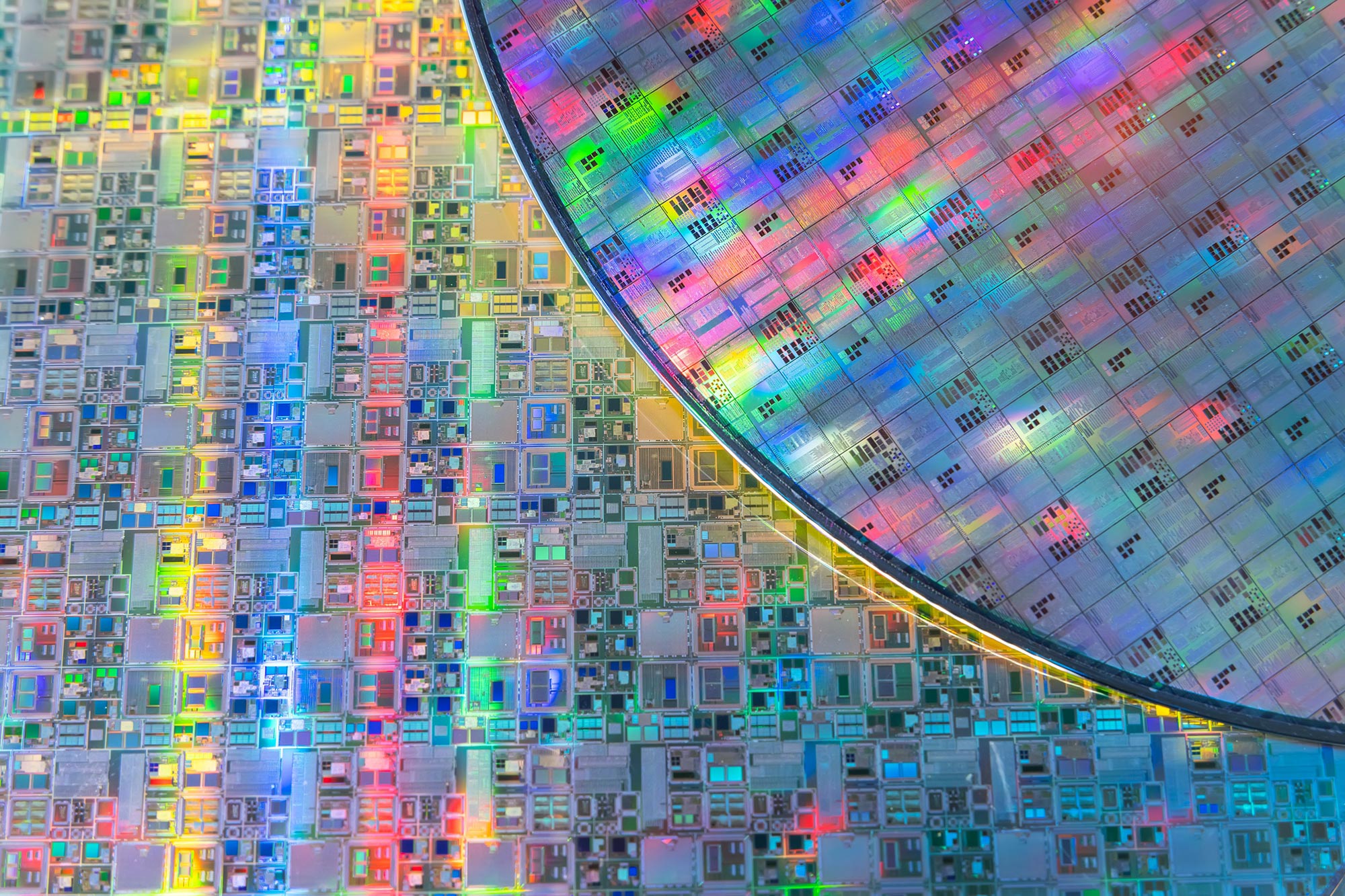
Scientists at Johns Hopkins have uncovered a new way to build microchips so small they’re nearly invisible.
By combining metals and light-sensitive chemistry, they’ve pioneered a method that could make chips faster, cheaper, and far more powerful. This leap in microchip design could reshape everything from smartphones to airplanes, opening a path to the next era of technology.
Breakthrough in Microchip Innovation
Researchers at Johns Hopkins have identified new materials and developed a new technique that could accelerate the race to produce microchips that are smaller, faster, and more affordable. These chips power nearly every corner of modern life, from smartphones and household appliances to automobiles and aircraft.
The scientists demonstrated how to build circuits so tiny they cannot be seen with the human eye, using a method designed to be both highly accurate and cost-effective for large-scale production.
The results of this research were published recently in Nature Chemical Engineering.
Overcoming Manufacturing Barriers
“Companies have their roadmaps of where they want to be in 10 to 20 years and beyond,” said Michael Tsapatsis, a Bloomberg Distinguished Professor of chemical and biomolecular engineering at Johns Hopkins University. “One hurdle has been finding a process for making smaller features in a production line where you irradiate materials quickly and with absolute precision to make the process economical.”
According to Tsapatsis, the advanced lasers required to etch patterns at these extremely small scales are already available. The missing piece has been the right materials and methods that can keep pace with the demand for ever smaller microchips.
How Microchips Are Made
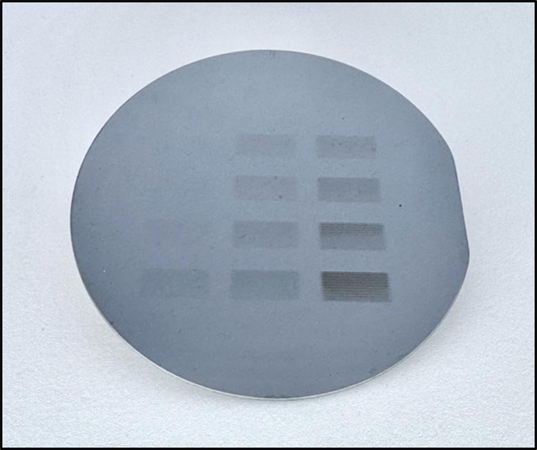
Microchips are flat pieces of silicon with imprinted circuitry that execute basic functions. During production, manufacturers coat silicon wafers with a radiation-sensitive material to create a very fine coating called a “resist.” When a beam of radiation is pointed at the resist, it sparks a chemical reaction that burns details into the wafer, drawing patterns and circuitry.
However, the higher-powered radiation beams that are needed to carve out ever-smaller details on chips do not interact strongly enough with traditional resists.
Pushing Past Current Limits
Previously, researchers from Tsapatsis’s lab and the Fairbrother Research Group at Johns Hopkins found that resists made of a new class of metal-organics can accommodate that higher-powered radiation process, called “beyond extreme ultraviolet radiation” (B-EUV), which has the potential to make details smaller than the current standard size of 10 nanometers. Metals like zinc absorb the B-EUV light and generate electrons that cause chemical transformations needed to imprint circuit patterns on an organic material called imidazole.
This research marks one of the first times scientists have been able to deposit these imidazole-based metal-organic resists from solution at silicon-wafer scale, controlling their thickness with nanometer precision. To develop the chemistry needed to coat the silicon wafer with the metal-organic materials, the team combined experiments and models from Johns Hopkins University, East China University of Science and Technology, École Polytechnique Fédérale de Lausanne, Soochow University, Brookhaven National Laboratory and Lawrence Berkeley National Laboratory. The new methodology, which they call chemical liquid deposition (CLD), can be precisely engineered and lets researchers quickly explore various combinations of metals and imidazoles.
“By playing with the two components (metal and imidazole), you can change the efficiency of absorbing the light and the chemistry of the following reactions. And that opens us up to creating new metal-organic pairings,” Tsapatsis said. “The exciting thing is there are at least 10 different metals that can be used for this chemistry, and hundreds of organics.”
Looking Ahead to Next-Gen Manufacturing
The researchers have started experimenting with different combinations to create pairings specifically for B-EUV radiation, which they say will likely be used in manufacturing in the next 10 years.
“Because different wavelengths have different interactions with different elements, a metal that is a loser in one wavelength can be a winner with the other,” Tsapatsis said. “Zinc is not very good for extreme ultraviolet radiation, but it’s one of the best for the B-EUV.”
Reference: “Spin-on deposition of amorphous zeolitic imidazolate framework films for lithography applications” by Yurun Miao, Shunyi Zheng, Kayley E. Waltz, Mueed Ahmad, Xinpei Zhou, Yegui Zhou, Heting Wang, J. Anibal Boscoboinik, Qi Liu, Kumar Varoon Agrawal, Oleg Kostko, Liwei Zhuang and Michael Tsapatsis, 11 September 2025, Nature Chemical Engineering.
DOI: 10.1038/s44286-025-00273-z
Authors include Yurun Miao, Kayley Waltz, and Xinpei Zhou from Johns Hopkins University; Liwei Zhuang, Shunyi Zheng, Yegui Zhou, and Heting Wang from East China University of Science and Technology; Mueed Ahmad and J. Anibal Boscoboinik from Brookhaven National Laboratory; Qi Liu from Soochow University; Kumar Varoon Agrawal from École Polytechnique Fédérale de Lausanne; and Oleg Kostko from Lawrence Berkeley National Laboratory.
Never miss a breakthrough: Join the SciTechDaily newsletter.
Follow us on Google and Google News.
2 Comments
So, finally something they can plant in our brains, eh?
“When a beam of radiation is pointed at the resist, it sparks a chemical reaction that burns details into the wafer, drawing patterns and circuitry.”
Oh!, so scientists at Johns Hopkins invented laser etching?!