A 2D Perspective: Stacking Materials to Realize a Low Power Consuming Future
Scientists have designed a 2D material-based multi-stacked structure comprising tungsten disulfide (WS2) layer sandwiched between hexagonal boron nitride (hBN) layers that displays long-range interaction between successive WS2 layers with potential for reducing circuit design complexity and power consumption.
2D materials have been popular among materials scientists owing to their lucrative electronic properties, allowing their applications in photovoltaics, semiconductors, and water purification. In particular, the relative physical and chemical stability of 2D materials allow them to be “stacked” and “integrated” with each other. In theory, this stability of 2D materials enables the fabrication of 2D material-based structures like coupled “quantum wells” (CQWs), a system of interacting potential “wells,” or regions holding very little energy, which allow only specific energies for the particles trapped within them.
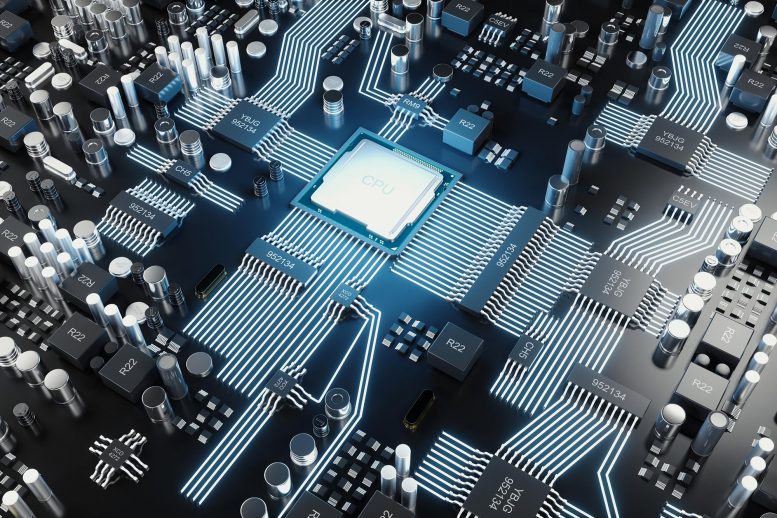
CQWs can be used to design resonant tunneling diodes, electronic devices that exhibit a negative rate of change of voltage with current and are crucial components of integrated circuits. Such chips and circuits are integral in technologies that emulate neurons and synapses responsible for memory storage in the biological brain.
Designing a CQW System with WS₂ and hBN
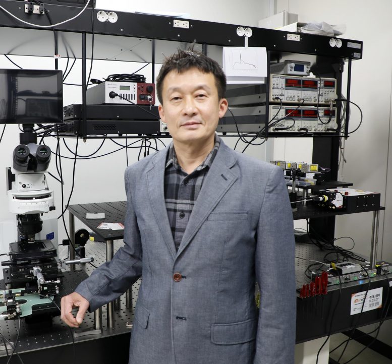
Proving that 2D materials can indeed be used to create CQWs, a research team led by Dr. Myoung-Jae Lee of Daegu Gyeongbuk Institute of Science and Technology (DGIST) designed a CQW system that stacks one tungsten disulfide (WS2) layer between two hexagonal boron nitride (hBN) layers. “hBN is a nearly ideal 2D insulator with high chemical stability. This makes it a perfect choice for integration with WS2, which is known to be a semiconductor in 2D form,” explains Prof. Lee. Their findings are in published in ACS Nano.
The team measured the energy of excitons—bound systems comprising an electron and an electron hole (absence of electron)—and trions (electron-bound exciton) for the CQW and compared them to that for bilayer WS2 structures to identify the effect of WS2-WS2 interaction. They also measured the current-voltage characteristics of a single CQW to characterize its behavior.
Resonant Tunneling Diode Behavior Confirmed
They observed a gradual decrease in both the exciton and trion energy with an increase in the number of stakes, and an abrupt decrease in the bilayer WS2. They attributed these observations to a long-range inter-well interaction and strong WS2-WS2 interactions in absence of hBN, respectively. The current-voltage characteristics confirmed that it behaves like a resonant tunneling diode.
So, what implications do these results have for the future of electronics? Prof. Lee summarizes, “We can use resonant tunneling diodes for making multivalued logic devices that will reduce circuit complexity and computing power consumptions considerably. This, in turn, can lead to the development of low-power electronics.”
These findings are sure to revolutionize the electronics industry with extreme low power semiconductor chips and circuits, but what is more exciting is where these chips can take us, as they can be employed in applications that mimic neurons and synapses, which play a role in memory storage in the biological brain. This “2D perspective” may thus be the next big thing in artificial intelligence!
Reference: “Measurement of Exciton and Trion Energies in Multistacked hBN/WS2 Coupled Quantum Wells for Resonant Tunneling Diodes” by Myoung-Jae Lee, David H. Seo, Sung Min Kwon, Dohun Kim and Youngwook Kim, 3 November 2020, ACS Nano.
DOI: 10.1021/acsnano.0c08133
Never miss a breakthrough: Join the SciTechDaily newsletter.
Follow us on Google and Google News.