
Researchers have discovered a method for creating new materials for use in batteries, magnets, and microelectronics.
The most skilled artists can create a one-of-a-kind masterpiece using just a few different colors of paint. They accomplish this by utilizing inspiration, past artistic knowledge, and principles learned through years of practice in the studio.
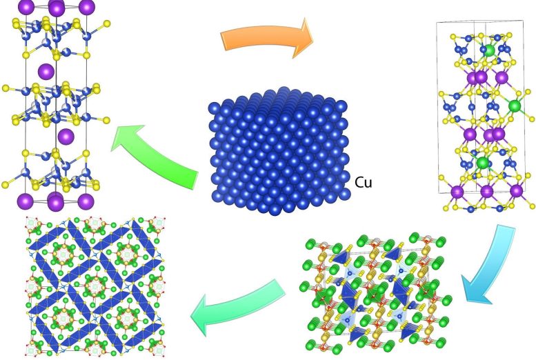
Chemists employ a similar process when developing new compounds. A team of researchers from the U.S. Department of Energy’s Argonne National Laboratory, Northwestern University, and The University of Chicago has created a new technique for identifying and synthesizing crystalline materials that contain two or more elements.
“We expect that our work will prove extremely valuable to the chemistry, materials, and condensed matter communities for synthesizing new and currently unpredictable materials with exotic properties,” said Mercouri Kanatzidis, a chemistry professor at Northwestern with a joint appointment at Argonne.
“Our invention method grew out of research on unconventional superconductors,” said Xiuquan Zhou, a postdoc at Argonne and the first author of the paper. “These are solids with two or more elements, at least one of which is not a metal. And they cease to resist the passage of electricity at different temperatures — anywhere from colder than outer space to that in my office.”
Over the last five decades, scientists have discovered and made many unconventional superconductors with surprising magnetic and electrical properties. Such materials have a wide gamut of possible applications, such as improved power generation, energy transmission, and high-speed transportation. They also have the potential for incorporation into future particle accelerators, magnetic resonance imaging systems, quantum computers, and energy-efficient microelectronics.
A Breakthrough Method for Material Synthesis
The team’s invention method starts with a solution made of two components. One is a highly effective solvent. It dissolves and reacts with any solids added to the solution. The other is not as good a solvent. But it is there for tuning the reaction to produce a new solid upon the addition of different elements. This tuning involves changing the ratio of the two components and the temperature. Here, the temperature is quite high, from 750 to 1,300 degrees Fahrenheit.
“We are not concerned with making known materials better but with discovering materials no one knew about or theorists imagined even existed,” Kanatzidis noted. “With this method, we can avoid reaction pathways to known materials and follow new paths into the unknown and unpredicted.”
Testing and Characterizing New Compounds
As a test case, the researchers applied their method to crystalline compounds made of three to five elements. As recently reported in Nature, their discovery method yielded 30 previously unknown compounds. Ten of them have structures never seen before.
The team prepared single crystals of some of these new compounds and characterized their structures at UChicago’s ChemMatCARS beamline at 15-ID-D and the X-ray Science Division’s 17-BM-B of the Advanced Photon Source, a DOE Office of Science user facility at Argonne. “With beamline 17-BM-B of the APS, we were able to track the evolution of the structures for the different chemical phases that formed during the reaction process,” said 17-BM-B beamline scientist Wenqian Xu.
“Traditionally, chemists have invented and made new materials relying only on knowledge of the starting ingredients and final product,” Zhou said. “The APS data allowed us to also take into account the intermediate products that form during a reaction.”
The Center for Nanoscale Materials, another DOE Office of Science user facility at Argonne, contributed key experimental data and theoretical calculations to the project.
And this is only the beginning of what is possible, since the method can be applied to almost any crystalline solid. It can also be applied to producing many different crystal structures. That includes multiple stacked layers, a single layer an atom thick, and chains of molecules that are not linked. Such unusual structures have different properties and are key to developing next-generation materials applicable to not only superconductors, but also microelectronics, batteries, magnets, and more.
Reference: “Discovery of chalcogenides structures and compositions using mixed fluxes” by Xiuquan Zhou, Venkata Surya Chaitanya Kolluru, Wenqian Xu, Luqing Wang, Tieyan Chang, Yu-Sheng Chen, Lei Yu, Jianguo Wen, Maria K. Y. Chan, Duck Young Chung and Mercouri G. Kanatzidis, 9 November 2022, Nature.
DOI: 10.1038/s41586-022-05307-7
The study was funded by the DOE’s Office of Science, Basic Energy Sciences program.
Never miss a breakthrough: Join the SciTechDaily newsletter.
Follow us on Google and Google News.