A novel device now enables scientists to easily adjust the twist between layers of ultra-thin materials, promising significant advances in electronics and optics. This could lead to better transistors and solar cells, and enhance research in quantum computing.
Six years ago, a groundbreaking discovery revolutionized condensed-matter physics: ultra-thin carbon layers, stacked at a slight angle, transformed into superconductors. By adjusting the twist angle between the layers, researchers found they could control the material’s electrical properties. This discovery, detailed in a landmark 2018 paper on “magic-angle graphene superlattices,” gave rise to a new field known as “twistronics.” The study’s first author was Yuan Cao, then a graduate student at MIT and later a Harvard Junior Fellow.
Building on this pioneering work, Cao, along with Harvard physicists Amir Yacoby, Eric Mazur, and their colleagues, developed a more efficient method to manipulate and study a wide range of materials, paving the way for further advancements in twistronics research.
Introducing MEGA2D: A New Tool for Material Manipulation
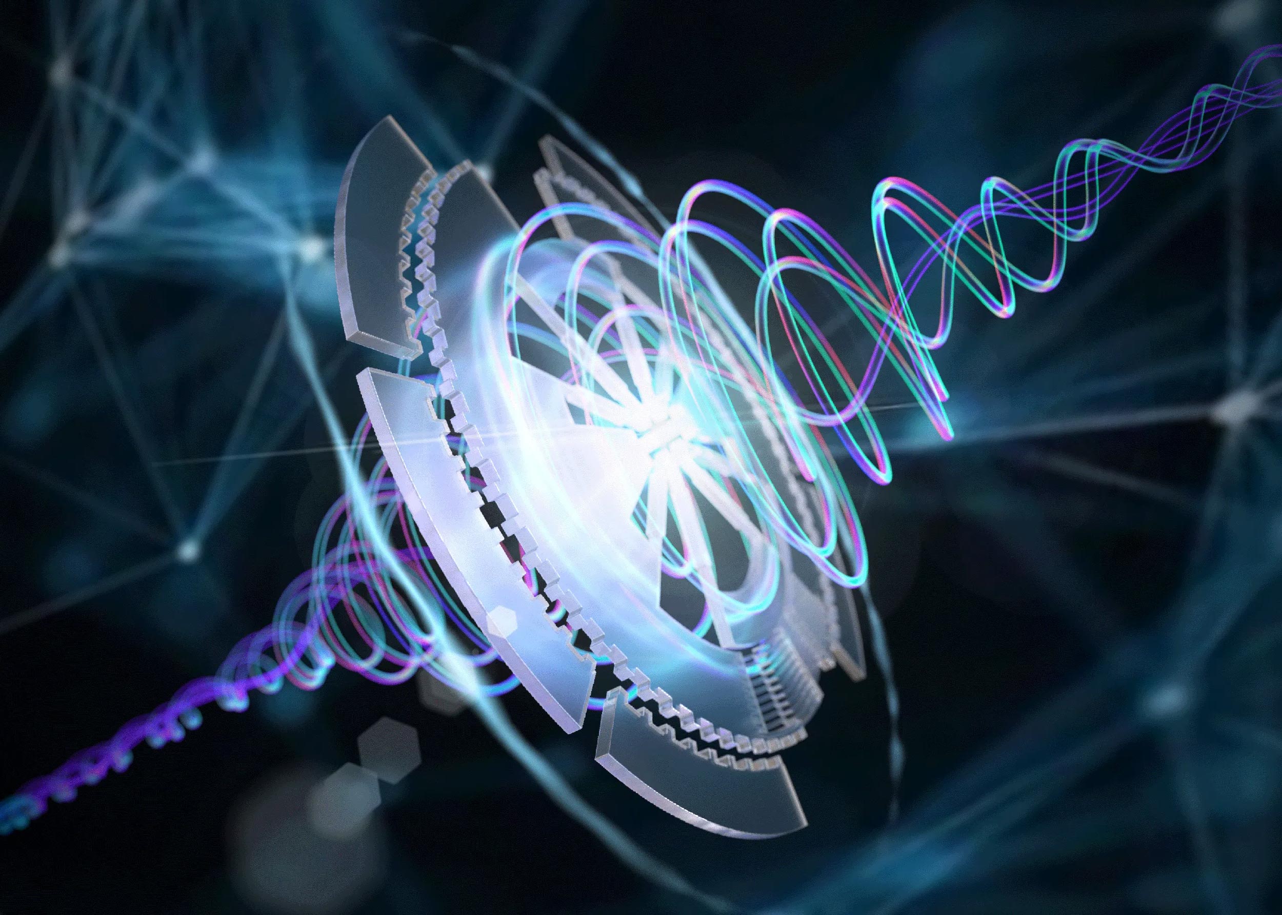
A new paper in Nature describes the team’s fingernail-sized machine that can twist thin materials at will, replacing the need to fabricate twisted devices one by one. Thin, 2D materials with properties that can be studied and manipulated easily have immense implications for higher-performance transistors, optical devices such as solar cells, and quantum computers, among other things.
“This development makes twisting as easy as controlling the electron density of 2D materials,” said Yacoby, Harvard professor of physics and applied physics. “Controlling density has been the primary knob for discovering new phases of matter in low-dimensional matter, and now, we can control both density and twist angle, opening endless possibilities for discovery.”
Challenges and Breakthroughs in Fabricating Twisted Devices
Cao first made twisted bilayer graphene as a graduate student in the lab of MIT’s Pablo Jarillo-Herrero. Exciting as it was, the achievement was tempered by challenges with replicating the actual twisting.
At the time, each twisted device was hard to produce, and as a result, unique and time-consuming, Cao explained. To do science with these devices, they needed tens or even hundreds of them. They wondered if they could make “one device to twist them all,” Cao said — a micromachine that could twist two layers of material at will, eliminating the need for hundreds of unique samples. They call their new device a MEMS (micro-electromechanical system)-based generic actuation platform for 2D materials, or MEGA2D for short.
Potential Applications and Future of Twistronics
The Yacoby and Mazur labs collaborated on the design of this new tool kit, which is generalizable to graphene and other materials.
“By having this new ‘knob’ via our MEGA2D technology, we envision that many underlying puzzles in twisted graphene and other materials could be resolved in a breeze,” said Cao, now an assistant professor at the University of California Berkeley. “It will certainly also bring other new discoveries along the way.”
In the paper, the researchers demonstrated the utility of their device with two pieces of hexagonal boron nitride, a close relative of graphene. They were able to study the bilayer device’s optical properties, finding evidence of quasiparticles with coveted topological properties.
The ease of their new system opens several scientific roadways, for example, employing hexagonal boron nitride twistronics to produce light sources that can be used for low-loss optical communication.
“We hope that our approach will be adopted by many other researchers in this prosperous field, and all can benefit from these new capabilities,” Cao said.
From Concept to Reality: Developing MEGA2D
The paper’s first author is nanoscience and optics expert Haoning Tang, a postdoctoral researcher in Mazur’s lab and a Harvard Quantum Initiative fellow, who noted that developing the MEGA2D technology was a long process of trial and error.
“We didn’t know much about how to control the interfaces of 2D materials in real time, and the existing methods just weren’t cutting it,” she said. “After spending countless hours in the cleanroom and refining the MEMS design — despite many failed attempts — we finally found the working solution after about a year of experiments.” All nanofabrication took place at Harvard’s Center for Nanoscale Systems, where staff provided invaluable technical support, Tang added.
Implications for Optics and Photonics
“The nanofabrication of a device combining MEMS technology with a bilayer structure is a veritable tour de force,” said Mazur, the Balkanski Professor of Physics and Applied Physics. “Being able to tune the nonlinear response of the resulting device opens the door to a whole new class of devices in optics and photonics.”
Reference: “On-chip multi-degree-of-freedom control of two-dimensional materials” by Haoning Tang, Yiting Wang, Xueqi Ni, Kenji Watanabe, Takashi Taniguchi, Pablo Jarillo-Herrero, Shanhui Fan, Eric Mazur, Amir Yacoby and Yuan Cao, 21 August 2024, Nature.
DOI: 10.1038/s41586-024-07826-x
Federal funding for the research was provided by the Defense Advanced Research Projects Agency, the Army Research Office, the U.S. Air Force Office of Scientific Research, and the National Science Foundation.
Never miss a breakthrough: Join the SciTechDaily newsletter.
Follow us on Google and Google News.
3 Comments
VERY GOOD!
Topological vortex theory (TVT) treats space as an ideal fluid, introduces the concept of topological phase transition, focuses on the topological properties and spatial structure of spacetime vortices, and profoundly describes the interconnection between time and space.
This theory not only changed our understanding of the state of matter and the structure of the universe, but also opened up new directions for future physics research. However, Developing the 2D technology was a long process of trial and error.
Incredible breakthrough—excited to see how this transforms material science! Tech frontiers at Verinae.
Fascinating innovation! MEGA2D could reshape how we use 2D materials—science is moving fast.