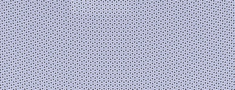
AMOLF researchers, in collaboration with Delft University of Technology, succeeded in bringing light waves to a halt by deforming the two-dimensional photonic crystal that contains them. The researchers showed that even a subtle deformation can have a substantial effect on photons in the crystal. This resembles the effect that a magnetic field has on electrons.
“This principle offers a new approach to slow down light fields and thereby enhance their strength. Realizing this on a chip is particularly important for many applications,” says AMOLF-group leader Ewold Verhagen. The researchers published their findings in the scientific journal Nature Photonics on April 23rd. Simultaneously, a research team from Pennsylvania State University published an article in this journal about how they demonstrated – independently from the Dutch team – an identical effect.
Manipulating the flow of light in a material at small scales is beneficial for the development of nanophotonic chips. For electrons such manipulation can be realized using magnetic fields; the Lorentz force steers the motion of electrons. However, this is impossible for photons because they do not have charge. Researchers in the Photonic Forces group at AMOLF are looking for techniques and materials that would enable them to apply forces to photons that resemble the effects of magnetic fields.
Electrons
“We looked for inspiration at the way in which electrons behave in materials. In a conductor, electrons can in principle move freely, but an external magnetic field can stop this. The circular movement caused by the magnetic field stops conduction and as such electrons can only exist in the material if they have very specific energies. These energy levels are called Landau levels, and they are characteristic for electrons in a magnetic field,” says Verhagen.
“But, in the two-dimensional material graphene – that consists of a single layer of carbon atoms arranged in a crystal – these Landau levels can also be caused by a different mechanism than a magnetic field. In general, graphene is a good electronic conductor, but this changes when the crystal array is deformed, for instance by stretching it like elastics. Such mechanical deformation stops conduction; the material turns into an insulator and consequently, the electrons are bound to Landau levels. Hence, the deformation of graphene has a similar effect on electrons in a material as a magnetic field, even without a magnet. We asked ourselves if a similar approach would also work for photons.”

Photonic Crystal
In a collaboration with Kobus Kuipers of Delft University of Technology, the group of Verhagen indeed demonstrated a similar effect for light in a photonic crystal. “A photonic crystal normally consists of a regular – two dimensional – pattern of holes in a silicon layer. Light can move freely in this material, just like electrons in graphene,” says first author René Barczyk who successfully defended his PhD thesis on this topic last year. “Breaking this regularity in exactly the right manner will deform the array and consequently lock the photons. This is how we create Landau levels for photons.”
In Landau levels light waves no longer move; they do not flow through the crystal but stand still. The researchers succeeded in demonstrating this, showing that the deformation of the crystal array has a similar effect on photons as a magnetic field on electrons.
Verhagen stated, “By playing with the deformation pattern, we even managed to establish various types of effective magnetic fields in one material. As a result, photons can move through certain parts of the material but not in others. Hence, these insights also provide new ways to steer light on a chip.”
Simultaneous Experiments
The work of Verhagen and his team was inspired by theoretical predictions of researchers at Pennsylvania State University and Columbia University.
Verhagen recalls: “When we were doing our first measurements, I happened to speak to one of the authors of this other study. When it turned out that they were also looking for experimental evidence of the effect, we decided not to compete in being first to publish but instead to submit the work simultaneously to the publisher. While some details in the approach differed, both teams were able to stop light waves from moving and observe Landau levels by deforming a two-dimensional photonic crystal.
“This brings on-chip applications closer,” says Verhagen. “If we can confine light at the nanoscale and bring it to a halt like this, its strength will be enhanced tremendously. And not only at one location, but over the entire crystal surface. Such light concentration is very important in nanophotonic devices, for example for the development of efficient lasers or quantum light sources.”
Reference: “Observation of Landau levels and chiral edge states in photonic crystals through pseudomagnetic fields induced by synthetic strain” by René Barczyk, L. Kuipers and Ewold Verhagen, 23 April 2024, Nature Photonics.
DOI: 10.1038/s41566-024-01412-3
Never miss a breakthrough: Join the SciTechDaily newsletter.
Follow us on Google and Google News.