Semiconductor devices are small components that manage the movement of electrons in contemporary electronic gadgets. They are essential for powering a wide range of high-tech products, including cell phones, laptops, and vehicle sensors, as well as cutting-edge medical devices. However, the presence of material impurities or variations in temperature can interfere with electron flow, causing instability.
But now, theoretical and experimental physicists from the Würzburg-Dresden Cluster of Excellence ct.qmat—Complexity and Topology in Quantum Matter have developed a semiconductor device from aluminum-gallium-arsenide (AlGaAs). This device’s electron flow, usually susceptible to interference, is safeguarded by a topological quantum phenomenon. This groundbreaking research was recently detailed in the esteemed journal Nature Physics.
“Thanks to the topological skin effect, all of the currents between the different contacts on the quantum semiconductor are unaffected by impurities or other external perturbations. This makes topological devices increasingly appealing for the semiconductor industry. They eliminate the need for the extremely high levels of material purity that currently drive up the costs of electronics manufacturing,” explains Professor Jeroen van den Brink, director of the Institute for Theoretical Solid State Physics at the Leibniz Institute for Solid State and Materials Research in Dresden (IFW) and a principal investigator of ct.qmat.
Topological quantum materials, known for their exceptional robustness, are ideally suited for power-intensive applications. “Our quantum semiconductor is both stable and yet highly accurate—a rare combination. This positions our topological device as a thrilling new option in sensor engineering.”
Extremely Robust and Ultra-Precise
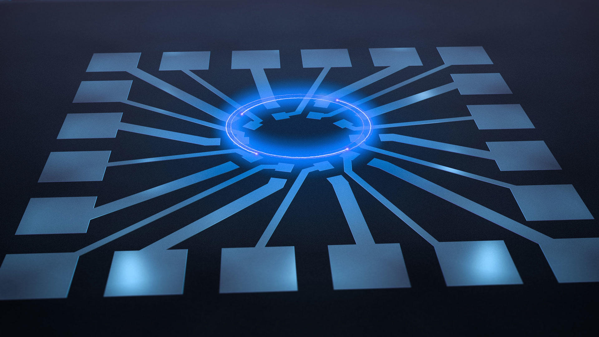
Utilizing the topological skin effect enables new types of high-performance electronic quantum devices that could also be incredibly small. “Our topological quantum device measures about 0.1 millimeters in diameter, and can be scaled down even further with ease,” reveals van den Brink. The pioneering aspect of this achievement by the team of physicists from Dresden and Würzburg is that they were the first to realize the topological skin effect on a microscopic scale in a semiconductor material. This quantum phenomenon was initially demonstrated at a macroscopic level three years ago—but only in an artificial metamaterial, not a natural one. This is therefore the first time that a tiny, semiconductor-based topological quantum device that’s both highly robust and ultra-sensitive has been developed.
“In our quantum device, the current–voltage relationship is protected by the topological skin effect because the electrons are confined to the edge. Even in the event of impurities in the semiconductor material, the current flow remains stable,” explains van den Brink. He continues: “Moreover, the contacts can detect even the slightest fluctuations in current or voltage. This makes the topological quantum device exceptionally well suited for making high-precision sensors and amplifiers with minuscule diameters.”
Innovative Experimentation Leads to Discovery
Success was achieved by creatively arranging materials and contacts on an AlGaAs semiconductor device, inducing the topological effect under ultra-cold conditions and a strong magnetic field. “We really coaxed the topological skin effect out of the device,” van den Brink explains. The physics team employed a two-dimensional semiconductor structure. The contacts were arranged in such a way that the electrical resistance could be measured at the contact edges, directly revealing the topological effect.
United Research in Different Locations
Since 2019, ct.qmat has been investigating topological quantum materials in Würzburg and Dresden, exploring their extraordinary behavior under extreme conditions like ultra-low temperatures, high pressures, or strong magnetic fields.
The recent breakthrough is also the result of sustained collaboration among scientists at the cluster’s two locations. The new quantum device, conceived at the IFW, was a joint effort involving theoretical physicists from Universität Würzburg as well as both theoretical and experimental researchers in Dresden. After being produced in France, the device was tested in Dresden. Jeroen van den Brink and his colleagues are now dedicated to further exploring this phenomenon, aiming to leverage it for future technological innovations.
Reference: “Non-Hermitian topology in a multi-terminal quantum Hall device” by Kyrylo Ochkan, Raghav Chaturvedi, Viktor Könye, Louis Veyrat, Romain Giraud, Dominique Mailly, Antonella Cavanna, Ulf Gennser, Ewelina M. Hankiewicz, Bernd Büchner, Jeroen van den Brink, Joseph Dufouleur and Ion Cosma Fulga, 18 January 2024, Nature Physics.
DOI: 10.1038/s41567-023-02337-4
Never miss a breakthrough: Join the SciTechDaily newsletter.
Follow us on Google and Google News.
2 Comments
The collaboration effect will surely lessen the negative approaches of pier review bring a regiment of agreement.
Question if u guys can do that would it not than be possible to build a space ship like the Enterprise with a quantan coreas its main power plant or do the lithium crystals still need to be the main power that drives the ship thank you for your time