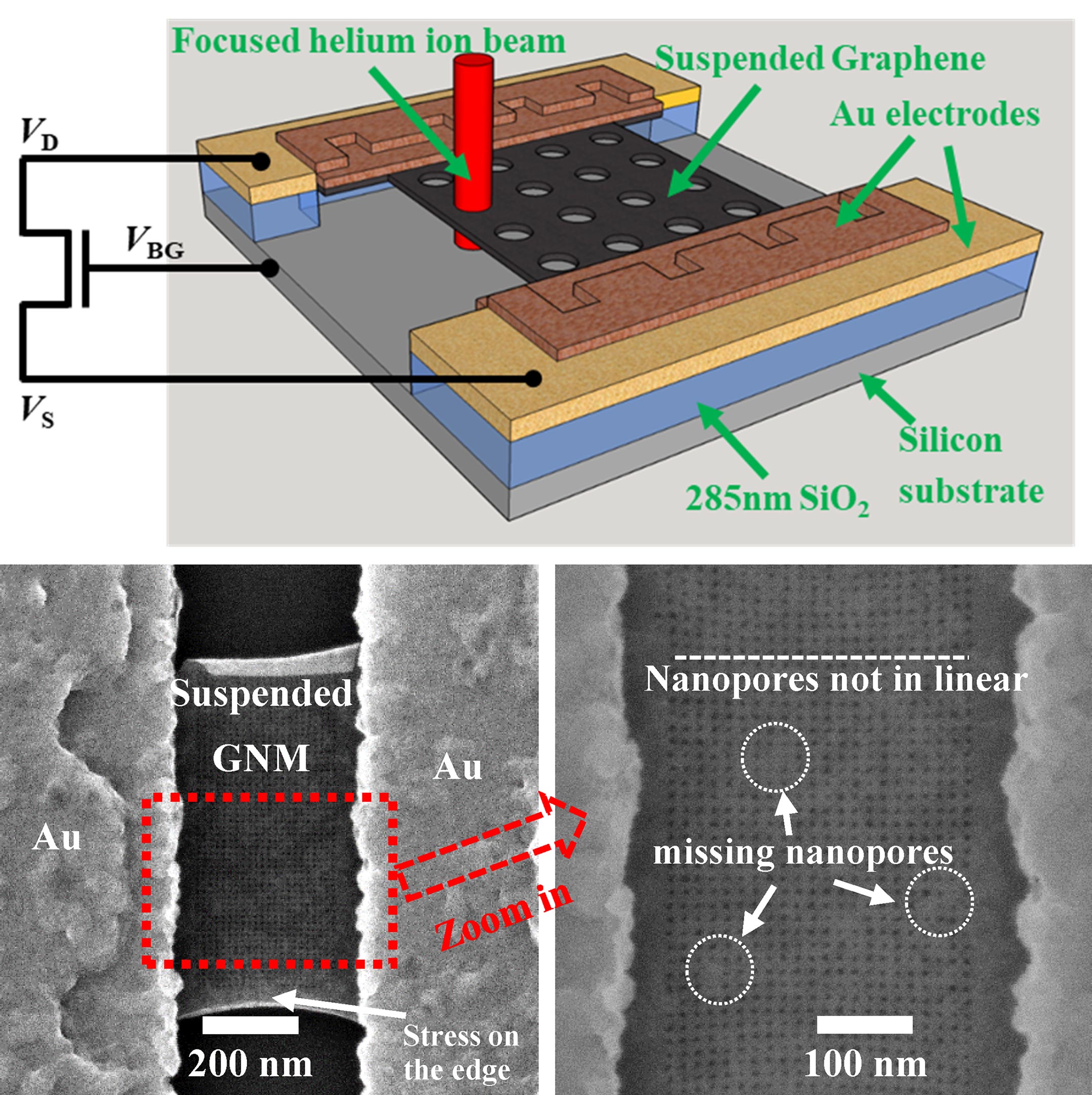
Researchers at the Japan Advanced Institute of Science and Technology (JAIST) have successfully fabricated a suspended graphene nanomesh over a large area using helium ion beam microscopy. 6nm diameter nanopores were patterned uniformly on the 1.2 um long and 500 nm wide suspended graphene. By systematically controlling the pitch (nanopore’s center to nanopore’s center) from 15 nm to 50 nm, a series of stable graphene nanomesh devices were achieved. This provides a practical way to investigate the intrinsic properties of graphene nanomesh towards the application for gas sensing, phonon engineering, and quantum technology.
Graphene, with its excellent electrical, thermal, and optical properties, is promising for many applications in the next decade. It is also a potential candidate for building the next generation of electrical circuits, instead of silicon. However, since graphene lacks a bandgap, it is not straightforward to use it as a field-effect transistor (FET). To address this issue, researchers have tried cutting the graphene sheet into small pieces of graphene nanoribbon, successfully opening up a bandgap. However, the current of graphene nanoribbons is too low to drive an integrated circuit. In this case, the graphene nanomesh is created by introducing periodic nanopores onto the graphene, which results in a very small array of graphene nanoribbons.
A research team led by Dr. Fayong Liu and Professor Hiroshi MIZUTA has demonstrated in collaboration with researchers at the National Institute of Advanced Industrial Science and Technology (AIST) that large-area suspended graphene nanomesh is quickly achievable by the helium ion beam microscopy with sub-10 nm nanopore diameter and well-controlled pitches. Comparing to slow-speed TEM patterning, the helium ion beam milling technique overcomes the speed limitation, and meanwhile, provides a high imaging resolution. With the initial electrical measurements, it has found that the thermal activation energy of the graphene nanomesh increased exponentially by increasing the porosity of the graphene nanomesh. This immediately provides a new method for bandgap engineering beyond the conventional nanoribbon method. The team plans to continue exploring graphene nanomesh toward the application of phonon engineering.
“Graphene nanomesh is a kind of new ‘brick’ for modern micromachine systems. Theoretically, we can generate many kinds of periodical patterns on the original suspended graphene, which tunes the property of the device to the direction for a special application, in particular nanoscale thermal management” says Prof. Hiroshi Mizuta, the Head of MIZUTA Lab. The MIZUTA lab is currently developing the electrical and thermal properties of graphene-based devices for fundamental physics and potential applications such as gas sensors and thermal rectifier. The aim is to use graphene to build a green world.
Reference: “Conductance Tunable Suspended Graphene Nanomesh by Helium Ion Beam Milling” by Fayong Liu, Zhongwang Wang, Soya Nakanao, Shinichi Ogawa, Yukinori Morita, Marek Schmidt, Mayeesha Haque, Manoharan Muruganathan and Hiroshi Mizuta, 7 April 2020, Micromachines.
DOI: 10.3390/mi11040387
This research was supported by the Grant in Aid for Scientific Research No. 18H03861, 19H05520 from the Japan Society for the Promotion of Science (JSPS).
Never miss a breakthrough: Join the SciTechDaily newsletter.
Follow us on Google and Google News.
1 Comment
to the local Facebook trolls being idiots again. Tosses another one at your heads being morons.