The U.S. Naval Research Laboratory (NRL), working together with Kansas State University, has announced the discovery of slab waveguides made from the two-dimensional material hexagonal boron nitride. This milestone has been documented in the journal Advanced Materials.
Two-dimensional (2D) materials are a class of materials that can be reduced to the monolayer limit by mechanically peeling the layers apart. The weak interlayer attractions, or van der Waals attraction, allows the layers to be separated via the so-called “Scotch tape” method. The most famous 2D material, graphene, is a semimetallic material consisting of a single layer of carbon atoms. Recently, other 2D materials including semiconducting transition metal dichalcogenides (TMDs) and insulating hexagonal boron nitride (hBN) have also garnered attention. When reduced near the monolayer limit, 2D materials have unique nanoscale properties that are appealing for creating atomically thin electronic and optical devices.
Unexpected Optical Properties
“We knew using hexagonal boron nitride would lead to outstanding optical properties in our samples, none of us expected that it would also act a waveguide,” said Samuel Lagasse, Ph.D., Novel Materials and Applications Division. “Since hBN is used so widely in 2D material–based devices, this novel usage as an optical waveguide potentially has wide-ranging impacts.“
Graphene and TMD monolayers are both extremely sensitive to the surrounding environment. Therefore, researchers have sought to protect these materials by encapsulating them in a passivating layer. This is where hBN comes in: layers of hBN are able to “screen” impurities near graphene or TMD layers, leading to fantastic properties. In recent NRL-led work, the thickness of hBN surrounding a light-emitting TMD layer was carefully tuned in order to support optical waveguide modes.
Advancements in Waveguide Technology
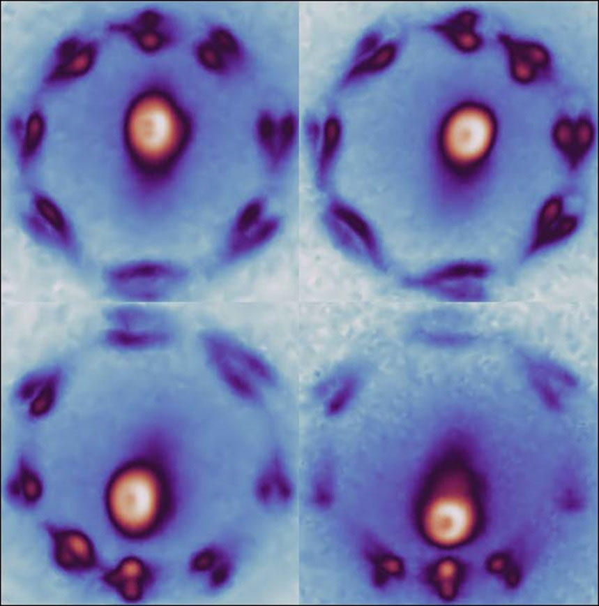
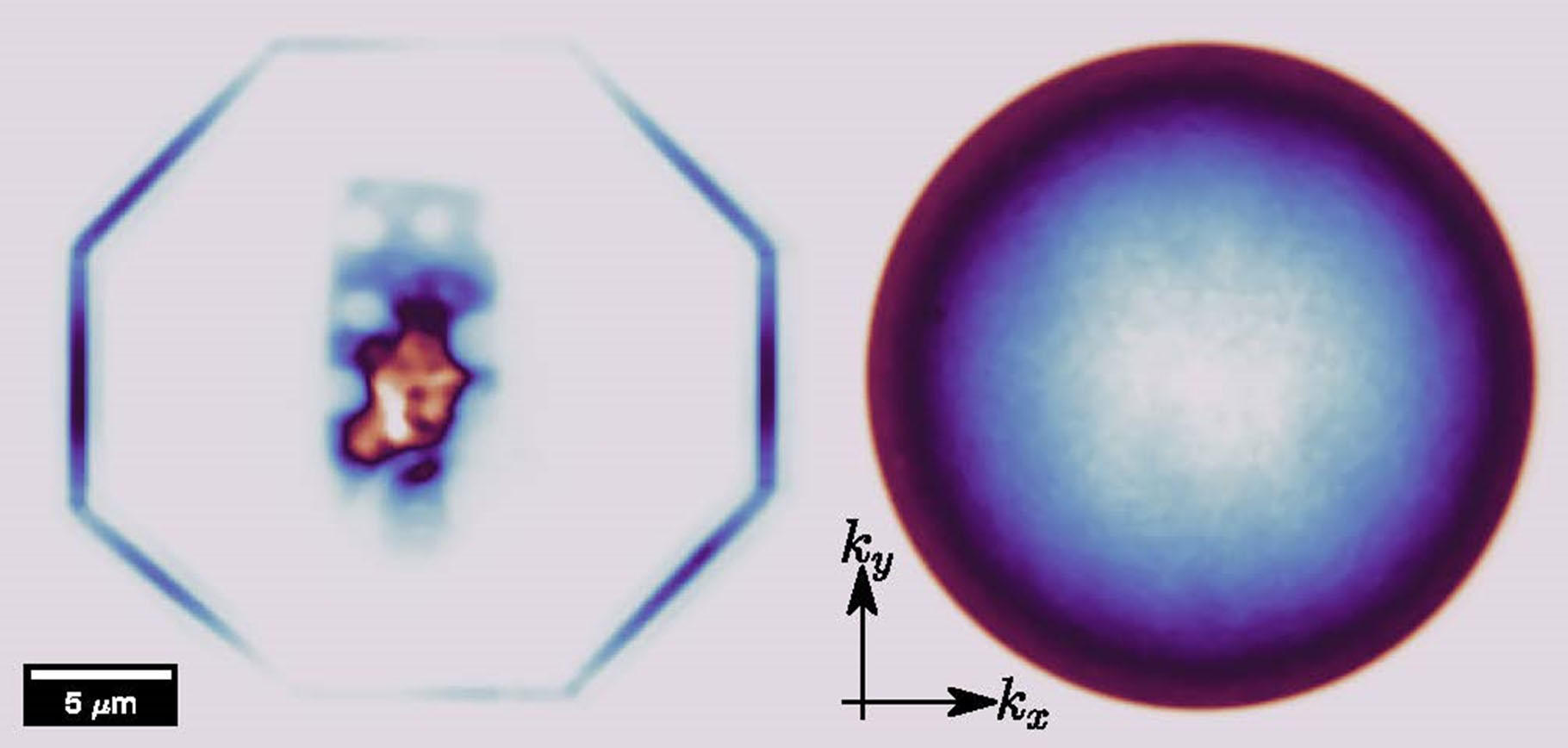
Researchers at NRL carefully assembled stacks of 2D materials, known as “van der Waals heterostructures.” These heterostructures can have specialized properties due to the layering. Slabs of hBN were placed around single layers of TMDs, such as molybdenum diselenide or tungsten diselenide, which can emit light in the visible and near-infrared. The slabs of hBN were carefully tuned in thickness so that the emitted light would be trapped within the hBN and waveguided. When the light waveguides to the edge of the hBN, it can scatter out and be detected by a microscope.
The research was motivated by the challenges of optical measurements of 2D TMDs. When laser light is focused on TMDs, particles known as excitons are generated. Most excitons emit light out of the plane of the TMD, however an elusive type of exciton known as a “dark” exciton exists in some TMDs, emits in the plane of the TMD. NRL’s slab waveguides capture the light from the dark excitons, providing a way to study them optically.
“2D materials have exotic optoelectronic properties that will be useful to the Navy,” said Lagasse. “A large challenge is interfacing these materials with existing platforms without damaging them – these boron nitride waveguides are a step towards that realization.”
NRL researchers used two special types of optical microscopes to characterize the hBN waveguides. One setup allows researchers to spectroscopically resolve photoluminescence emitting from different spots of the waveguide. The other setup let them observe the angular distribution of the emitted light.
NRL researchers also developed 3D electromagnetic models of the waveguides. The modeling results provide a toolkit for designing future 2D devices that use slab waveguides.
Reference: “Hexagonal Boron Nitride Slab Waveguides for Enhanced Spectroscopy of Encapsulated 2D Materials” by Samuel W. LaGasse, Nicholas V. Proscia, Cory D. Cress, Jose J. Fonseca, Paul D. Cunningham, Eli Janzen, James H. Edgar, Daniel J. Pennachio, James Culbertson, Maxim Zalalutdinov and Jeremy T. Robinson, 22 November 2023, Advanced Materials.
DOI: 10.1002/adma.202309777
Never miss a breakthrough: Join the SciTechDaily newsletter.
Follow us on Google and Google News.