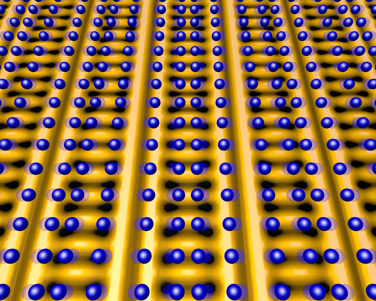
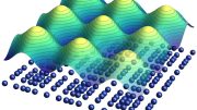
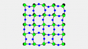
This image shows the positions of atoms (blue spheres) that make up the crystal lattice of a copper-oxide superconductor, superimposed on a map of electronic charge distribution (yellow is high charge density, dark spots are low) in charge-ordered states. Normally, the atoms can vibrate side-to-side (shadows represent average locations when vibrating). But when cooled to the point where the ladder-like charge density wave appears, the atomic positions shift along the “rungs” and the vibrations cease, locking the atoms in place. Understanding these charge-ordered states may help scientists unlock other interactions that trigger superconductivity at lower temperatures. Credit: Brookhaven National Laboratory
Precision measurements reveal connection between electron density and atomic arrangements in charge-ordered states of a superconducting copper-oxide material.
Researchers at the Brookhaven National Laboratory have discovered a direct connection between the disappearance of certain atomic vibrations and the emergence of a “charge density wave” in superconducting copper-oxide materials. This discovery, achieved through precision measurement, uncovers a vital relationship between atomic structure and charge distribution, advancing our understanding of superconductivity.
What makes some materials carry current with no resistance? Scientists are trying to unravel the complex characteristics. Harnessing this property, known as superconductivity, could lead to perfectly efficient power lines, ultrafast computers, and a range of energy-saving advances. Understanding these materials when they aren’t superconducting is a key part of the quest to unlock that potential.
“To solve the problem, we need to understand the many phases of these materials,” said Kazuhiro Fujita, a physicist in the Condensed Matter Physics & Materials Science Department of the U.S. Department of Energy’s Brookhaven National Laboratory. In a new study published on May 17 in Physical Review X, Fujita and his colleagues sought to find an explanation for an oddity observed in a phase that coexists with the superconducting phase of a copper-oxide superconductor.
The anomaly was a mysterious disappearance of vibrational energy from the atoms that make up the material’s crystal lattice. “X-rays show that the atoms vibrate in particular ways,” Fujita said. But as the material is cooled, the x-ray studies showed, one mode of the vibrations stops.
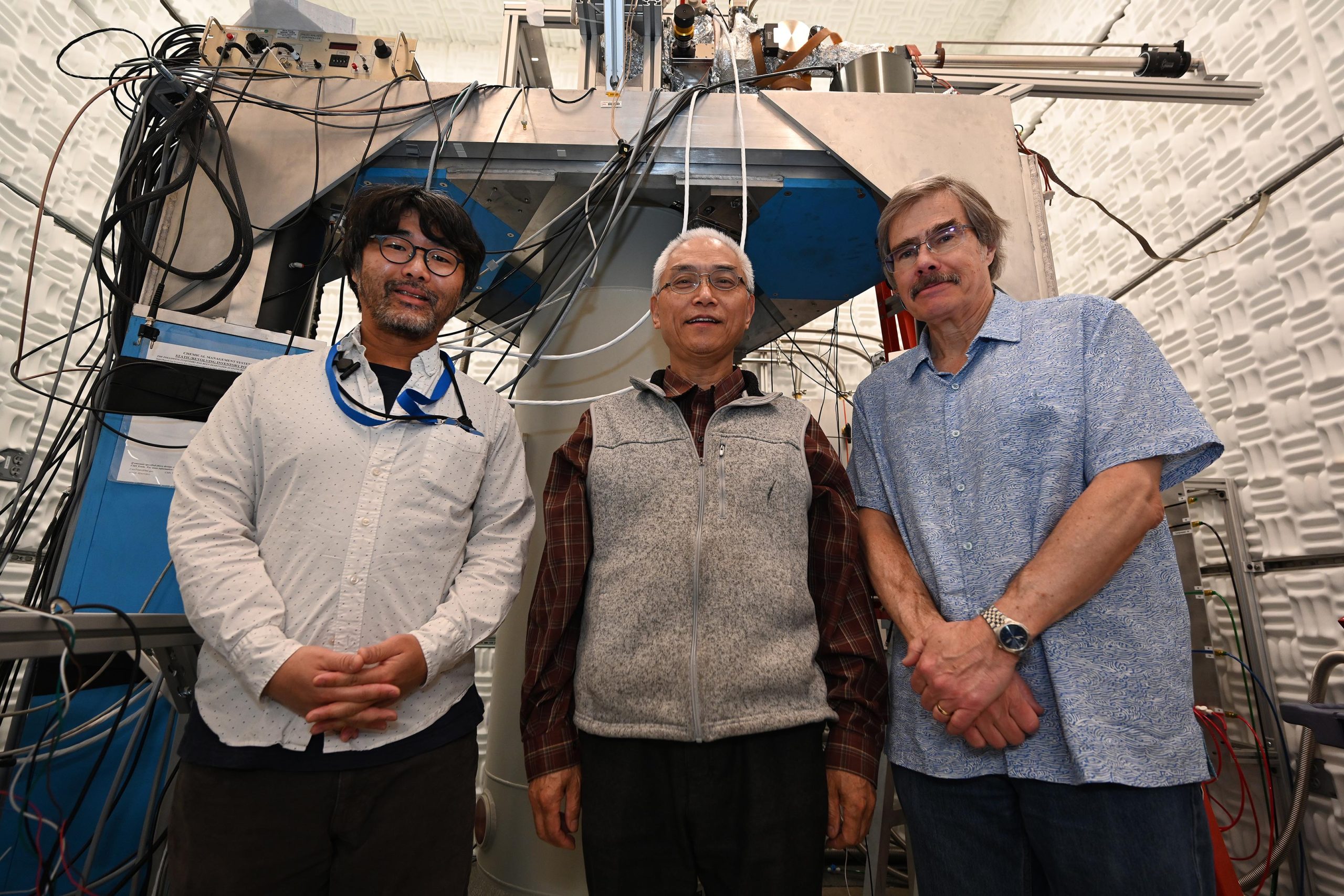
Kazuhiro Fujita (left) with Brookhaven Lab co-authors Genda Gu and John Tranquada, all members of Brookhaven Lab’s Condensed Matter Physics and Materials Science Department, in front of the spectroscopic imaging scanning tunneling microscope (SI-STM) used in this study. Credit: Brookhaven National Laboratory
“Our study explored the relationship between the lattice structure and the electronic structure of this material to see if we could understand what was going on,” Fujita said.
The Brookhaven team used a tool called a spectroscopic imaging scanning tunneling microscope (SI-STM). By scanning the surface of the layered material with trillionths-of-a-meter precision, they could map the atoms and measure the distances between them—while simultaneously measuring the electric charge at each atomic-scale location.
The measurements were sensitive enough to pick up the average positions of the atoms when they were vibrating—and showed how those positions shifted and became locked in place when the vibrations stopped. They also showed that the anomalous vibrational disappearance was directly linked to the emergence of a “charge density wave”—a modular distribution of charge density in the material.
The electrons that make up the charge density wave are localized, meaning in fixed positions—and separate from the more mobile electrons that eventually carry the current in the superconducting phase, Fujita explained. These localized electrons form a repeating pattern of higher and lower densities that can be visualized as ladders laying side-by-side (see diagram). It’s the appearance of this pattern that distorts the normal vibrations of the atoms and shifts their positions along the direction of the “rungs.”
“As the temperature goes down and the charge density wave (CDW) emerges, the vibrational energy goes down,” Fujita said. “By measuring both charge distribution and atomic structure simultaneously, you can see how the emergence of the CDW locks the atoms in place.”
“This result implies that, as the atoms vibrate, the charge density wave interacts with the lattice and quenches the lattice. It stops the vibrations and distorts the lattice,” Fujita said.
So that’s one more clue about how two of the characteristics of one phase of a superconducting material couple together. But there’s still a lot to uncover about these promising materials, Fujita said.
“There are many variables. Electrons and the lattice are just two. We have to consider all of these and how they interact with each other to truly understand these materials,” he said.
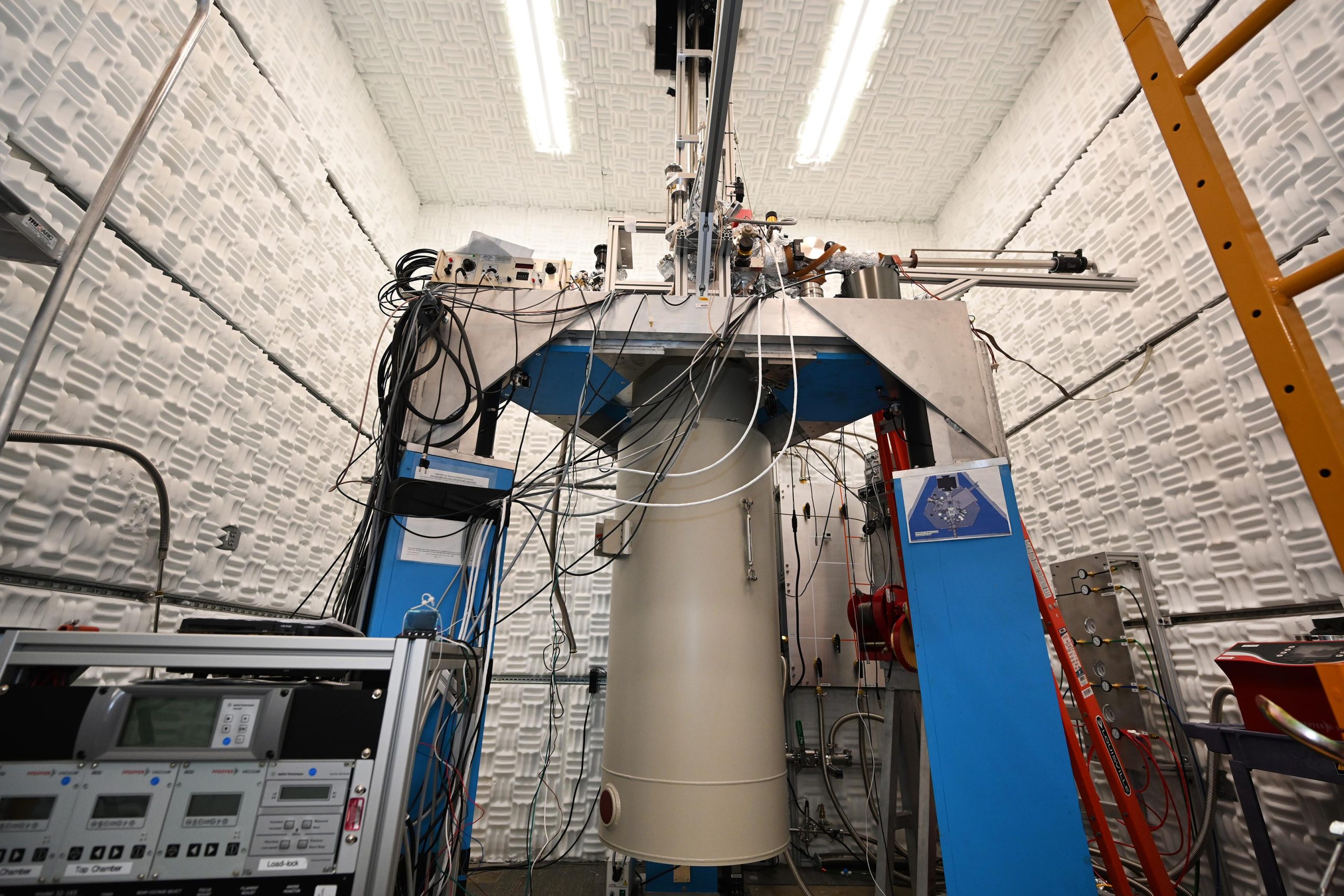
The spectroscopic imaging scanning tunneling microscope (SI-STM) used in this study at Brookhaven National Laboratory. Credit: Brookhaven National Laboratory
Precision atomic and electronic scanning
The spectroscopic imaging scanning tunneling microscope (SI-STM) used in this study achieves its extreme precision by being completely isolated from its surroundings. It’s situated in a cube of concrete that “floats” on vibration-cushioning springs anchored to the ground separately from the foundation of the Interdisciplinary Science Building on Brookhaven’s campus. An electromagnetically isolating Faraday cage, sound-insulating foam, and three layers of doors provide complete protection from any external vibrations.
“If there is any external vibration, that is going to kill the experiment,” Fujita said. “We need vibration isolation to perform the experiment correctly.”
When making measurements, a needle hovers over the sample at a distance of about one angstrom—one ten-billionth of a meter, or about the diameter of an atom—but not touching the surface. Applying varying voltages allows electrons to tunnel (or jump) from the sample to the tip, creating a current. The strength of the current at each location maps out the material’s electron density while simultaneous spectroscopic imaging captures the sample’s topographical features—including atomic positions and variations caused by impurities and imperfections.
Reference: “Periodic Atomic Displacements and Visualization of the Electron-Lattice Interaction in the Cuprate” by Zengyi Du, Hui Li, Genda Gu, Abhay N. Pasupathy, John M. Tranquada and Kazuhiro Fujita, 17 May 2023, Physical Review X.
DOI: 10.1103/PhysRevX.13.021025
This work was supported by the DOE Office of Science (BES).


The quest for a superconductor at ambient temperature could stand in lining up of the materials quantum makeup, then compressing the material to a very dense composition , reducing the exchange reaction distance between electrons / quirks for transfer of conduction.