For the first time, scientists electrically manipulate a ‘chiral interface state’ in a 2D material, with promise for energy-efficient microelectronics and quantum computing.
- Scientists have taken the first atomic-resolution images of an exotic quantum phenomenon that could help researchers advance quantum computing and energy-efficient electronics.
- The work enables the visualization and control of electron flow in a unique class of quantum insulators.
- The findings may help researchers build tunable networks of electron channels with promise for efficient quantum computing and low-power magnetic memory devices in the future.
Breakthrough in Quantum Computing and Electronics
An international research team led by Lawrence Berkeley National Laboratory (Berkeley Lab) has taken the first atomic-resolution images and demonstrated electrical control of a chiral interface state – an exotic quantum phenomenon that could help researchers advance quantum computing and energy-efficient electronics.
Unveiling Chiral Interface States
The chiral interface state is a conducting channel that allows electrons to travel in only one direction, preventing them from being scattered backward and causing energy-wasting electrical resistance. Researchers are working to better understand the properties of chiral interface states in real materials but visualizing their spatial characteristics has proved to be exceptionally difficult.
But now, for the first time, atomic-resolution images captured by a research team at Berkeley Lab and UC Berkeley have directly visualized a chiral interface state. The researchers also demonstrated on-demand creation of these resistance-free conducting channels in a 2D insulator.
Advancing Quantum Material Applications
Their work, which was reported in the journal Nature Physics, is part of Berkeley Lab’s broader push to advance quantum computing and other quantum information system applications, including the design and synthesis of quantum materials to address pressing technological needs.
“Our work shows for the first time what these 1D states look like at the atomic scale, including how we can alter them – and even create them.”
Canxun Zhang, former graduate student researcher, Materials Sciences Division
“Previous experiments have demonstrated that chiral interface states exist, but no one has ever visualized them with such high resolution. Our work shows for the first time what these 1D states look like at the atomic scale, including how we can alter them – and even create them,” said first author Canxun Zhang, a former graduate student researcher in Berkeley Lab’s Materials Sciences Division and the Department of Physics at UC Berkeley. He is now a postdoctoral researcher at UC Santa Barbara.
Innovative Techniques and Future Applications
Chiral interface states can occur in certain types of 2D materials known as quantum anomalous Hall (QAH) insulators that are insulators in bulk but conduct electrons without resistance at one-dimensional “edges” – the physical boundaries of the material and interfaces with other materials.
To prepare chiral interface states, the team worked at Berkeley Lab’s Molecular Foundry to fabricate a device called twisted monolayer-bilayer graphene, which is a stack of two atomically thin layers of graphene rotated precisely relative to one another, creating a moiré superlattice that exhibits the QAH effect.
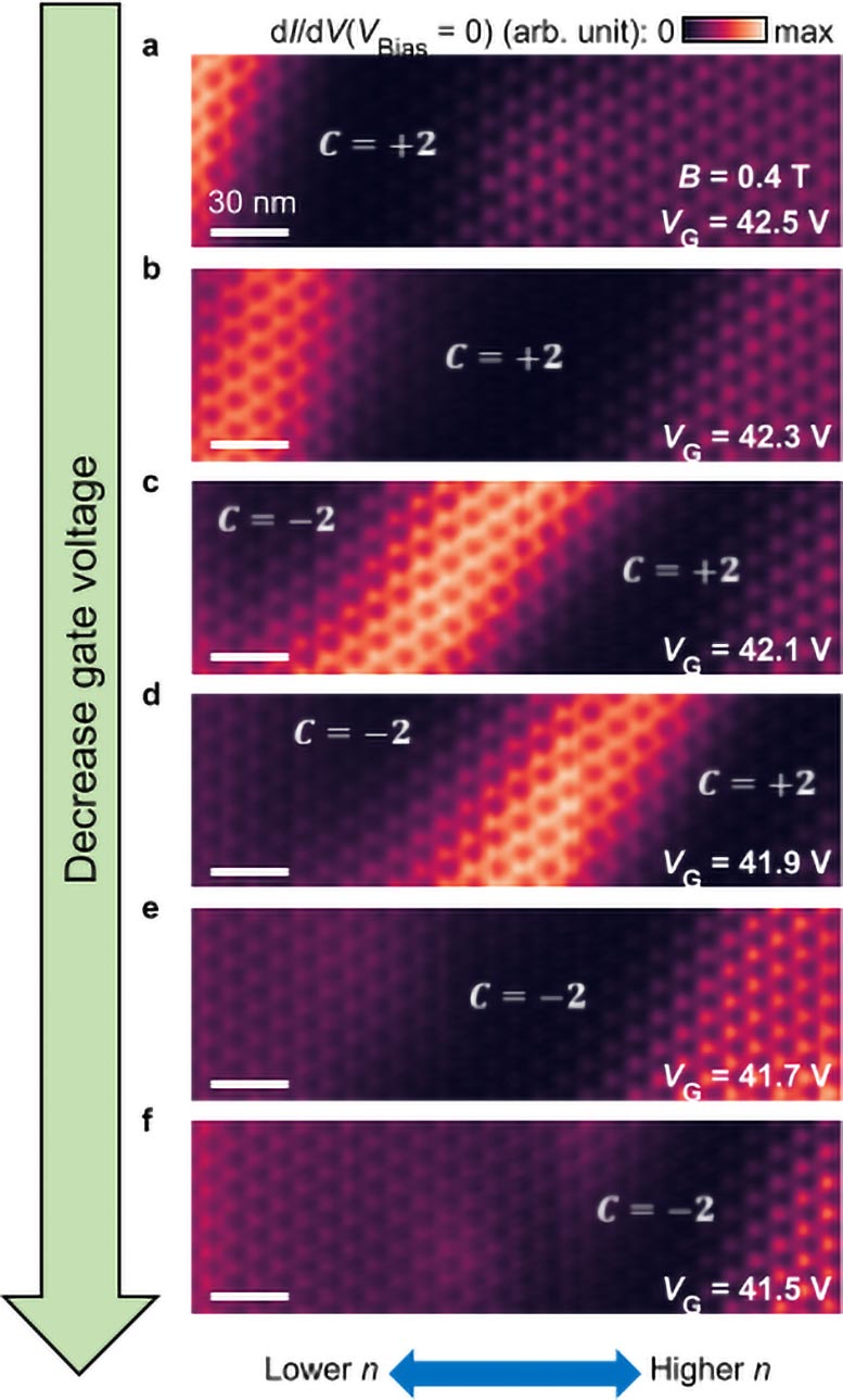
In subsequent experiments at the UC Berkeley Department of Physics, the researchers used a scanning tunneling microscope (STM) to detect different electronic states in the sample, allowing them to visualize the wavefunction of the chiral interface state. Other experiments showed that the chiral interface state can be moved across the sample by modulating the voltage on a gate electrode placed underneath the graphene layers. In a final demonstration of control, the researchers showed that a voltage pulse from the tip of an STM probe can “write” a chiral interface state into the sample, erase it, and even rewrite a new one where electrons flow in the opposite direction.
Potential Impact and Ongoing Research
The findings may help researchers build tunable networks of electron channels with promise for energy-efficient microelectronics and low-power magnetic memory devices in the future, and for quantum computation making use of the exotic electron behaviors in QAH insulators.
The researchers intend to use their technique to study more exotic physics in related materials, such as anyons, a new type of quasiparticle that could enable a route to quantum computation.
“Our results provide information that wasn’t possible before. There is still a long way to go, but this is a good first step,” Zhang said.
Reference: “Manipulation of chiral interface states in a moiré quantum anomalous Hall insulator” by Canxun Zhang, Tiancong Zhu, Salman Kahn, Tomohiro Soejima, Kenji Watanabe, Takashi Taniguchi, Alex Zettl, Feng Wang, Michael P. Zaletel and Michael F. Crommie, 13 March 2024, Nature Physics.
DOI: 10.1038/s41567-024-02444-w
The work was led by Michael Crommie, a senior faculty scientist in Berkeley Lab’s Materials Sciences Division and physics professor at UC Berkeley.
Tiancong Zhu, a former postdoctoral researcher in the Crommie group at Berkeley Lab and UC Berkeley, contributed as co-corresponding author and is now a physics professor at Purdue University.
The Molecular Foundry is a DOE Office of Science user facility at Berkeley Lab.
This work was supported by the DOE Office of Science. Additional funding was provided by the National Science Foundation.
Never miss a breakthrough: Join the SciTechDaily newsletter.
Follow us on Google and Google News.
1 Comment
Assuming the voltage as direct current, what would happen at a alternating current.