Scientists have developed a method to analyze the internal structures of vertically stacked two-dimensional materials, revealing atomic reconstructions that influence physical properties. This research holds promise for advancing our understanding and application of twisted electronics.
Vertically stacking two-dimensional (2D) materials to form van der Waals homo- or hetero-structure has become an effective means for regulating their physical and mechanical properties. In particular, when a small twist angle is present at the stacked interface, the 2D structures often show many interesting and even magical physical phenomena owing to the unique interlayer coupling.
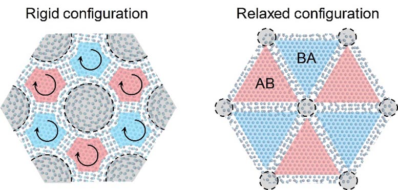
In the case of bilayer graphene with a small twist angle, the twisted interface will undergo spontaneous atomic reconstruction due to the competition between the interlayer stacking energy and the intralayer elastic strain energy, as schematically shown in Figure 1.
This special stacked structure can lead to many unexpected phenomena, including Mott insulating state, unconventional superconductivity and spontaneous ferromagnetism. Recently, it has been found that twisted interfaces can not only appear in the surface layer, but also can be embedded inside the van der Waals structures, which may lead to richer physical behaviors.
For these interesting 2D architectures, their physical properties are highly sensitive to the stacking state of the internal layers and interfaces. Unfortunately, how to precisely characterize the embedded stacking structure is still a grant challenge so far. In addition, whether the embedded twisted interfaces would also undergo atomic reconstruction and what impacts the reconstruction may have on the neighboring atomic layers as well as the whole stacked units are scientifically intriguing and remain unexplored.
Breakthrough Research
To answer these questions, Professor Qunyang Li’s group at Tsinghua University and Professor Ouyang Wengen’s group at Wuhan University have developed a new method based on conductive atomic force microscopy (c-AFM) to characterize and reconstruct the internal stacking state of twisted layered material through simple surface conductivity measurements. The related work has been published in National Science Review.
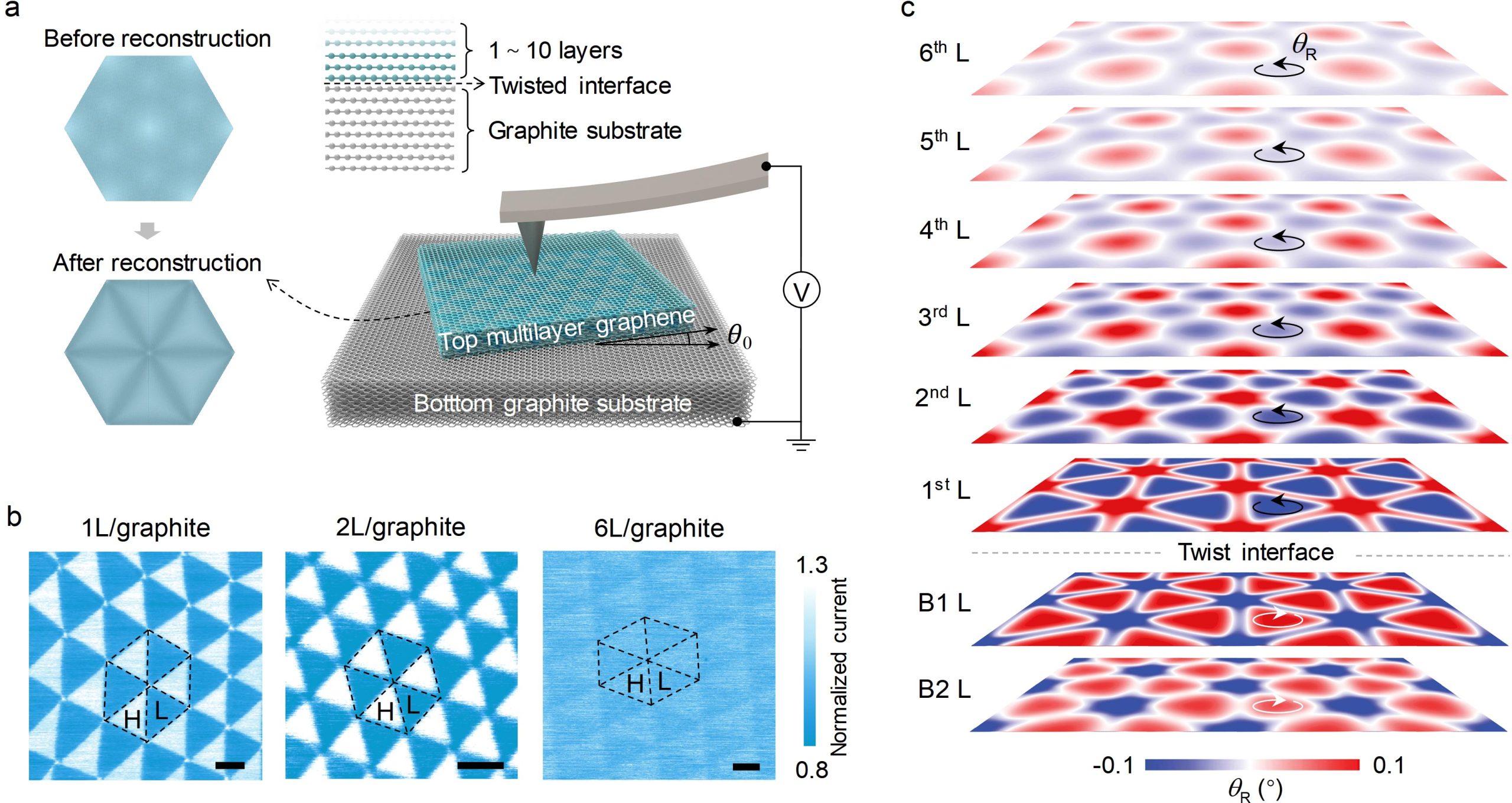
Their experimental results have shown that the twisted interfaces can still undergo atomic reconstruction and notably affect the surface conductivity even when they are embedded 10 atomic layers beneath the surface, as shown in Figure 2.
To better understand the atomic structure of the twisted multilayer system, a multilayer graphene system similar to the experimental samples has been constructed in a molecular dynamics (MD) simulation model by accurately considering the interlayer interactions. The simulation results have revealed that for small-angle twisted interfaces embedded in the interior of material, atomic reconstruction can indeed occur and promote the in-plane rotational deformation of the adjacent graphene layers. However, the atomic rotational deformation of graphene layer gradually decays as they are away from the twisted interface, as shown in Figure 2.
Proposed Model and Its Implications
Based on the atomic structures revealed in MD simulations, the research group proposed a series spreading resistance model (SSR model) to quantify the influence of the stacking state of twisted multilayer system on its surface conductivity. The new model enables a correlation between the surface conductivity and the internal stacking structure to be made directly, which is applicable even for twisted multilayer samples with complex crystal defects (e.g., dislocations).
This research provides a simple, convenient, and high-resolution means to characterize the internal stacking structures of twisted layered materials, which is crucial for fundamental studies of 2D stacked structures and the development of emerging twisted electronics.
Reference: “Deducing the internal interfaces of twisted multilayer graphene via moiré-regulated surface conductivity” by Huan Wang, Sen Wang, Shuai Zhang, Mengzhen Zhu, Wengen Ouyang and Qunyang Li, 19 June 2023, National Science Review.
DOI: 10.1093/nsr/nwad175
Never miss a breakthrough: Join the SciTechDaily newsletter.
Follow us on Google and Google News.
2 Comments
Two dimensional spatiotemporal matter is the foundation of high-dimensional spatiotemporal matter. Topological vortices are point defects in two-dimensional spacetime. Twist & Stack of Topological Vortices: The Foundation of Magic in 2D Materials. Please believe in topological vortex gravitational field theory. Good luck to you all!
I’m thinking the geometry has the key opening up imagination leads invention, just a thought about Dark matter the clumping in space has a comparative of cataracts in the human eye the clumps of proteins in the lens create a blurring affect if Dark matter clumps with no attractive charge, then maybe it a glueing of companion particles when they touch they adhere and over time grow.